Welcome to Laser Pointer Forums - discuss green laser pointers, blue laser pointers, and all types of lasers

Buy Site Supporter Role (remove some ads) | LPF Donations

Links below open in new window

FrozenGate by Avery

Tesla Coil Build Thread

Too bad it doesn't merge them into a single trace for differential, but that pic shows what I needed. Driver looks to be fine.

Now then, the next test would be to connect the GDT to the driver and scope the secondaries. This can be with the gdt disconnected or connected to the fets, as long as all the fets are good. Time to check the GDT, either way!


Alright so, my next order of operation is:
leave 555 timer connected to driver-power timer and driver-with the GDT connected to driver, scope Gate drive transformer secondaries with duel channels.
Should I expect to see a 12v square wave at 4.5kHz? What will a failure look like? A choppy or saw tooth wave?
If one channel is NOT inverted will I see an inverted wf on the scope?

On the secondaries do I affix one probe and ground to the corresponding secondary or does the ground stay at pin one. Is impedance going to be an issue here?
 
Last edited:
Both channels on the scope should be non inverted and one waveform should be inverted to the other .
 
Yes in the photo one one channel was inverted to the other. When I tested pin 6/7 I connected the ground clips to the (-) pin on the board rectifier.

I'm not exactly sure how to attach full res images to a thumb nail. Hope you can see what you need to here.
I got this wave form too
Maybe a mistaken pin

Good to finally see the schematic; looks exactly like what I thought it would be from looking at the photos. Your scope shots are fine (the recent one shows the invert as off) so it's what you should be expecting. By the way this is about *as simple* as any circuit can be (not just for coils but any circuit in general! - it's basically a 3 component circuit and 2 of them gate drivers are basically the same with one inverted) so I highly recommend you read the datasheets of each component and understand -exactly- what each of the signal lines should look like.

Sig, the toroid with 15 turns sounds just fine for 200kHz operation, but it will saturate around 42kHz at 0.2T flux saturation density as a limit.

Some comments on the schematic:
1. I still don't understand why the MUR1560s are necessary
2. You should add some reverse diodes across the gate resistors (e.g. 1N5819) I'm pretty sure you will be seeing some pretty severe shoot-through during each transition since there is no dead time.
3. MUR860s need to be soldered as CLOSE as possible to the MOSFET.

DwU, check out this schematic pioneered by Steve Ward for a very basic SSTC
http://www.stevehv.4hv.org/SSTC5/miniSSTCfnlsch.JPG

It's essentially the same but uses the 5V 74HC version of the inverter. It also has a very simply 555 interrupter circuit which I encourage you to put together, which acts as the interrupter.

See this page for more information: The Mini SSTC

The only thing I would change in that design (it's from 2007) is to swap out the IRFP460 FETs for something newer, and the reverse diodes. The big TO264 fets you have here are a pretty good if not a bit expensive part.

Alright so, my next order of operation is:
leave 555 timer connected to driver-power timer and driver-with the GDT connected to driver, scope Gate drive transformer secondaries with duel channels.
Should I expect to see a 12v square wave at 4.5kHz? What will a failure look like? A choppy or saw tooth wave?
If one channel is NOT inverted will I see an inverted wf on the scope?

On the secondaries do I affix one probe and ground to the corresponding secondary or does the ground stay at pin one. Is impedance going to be an issue here?

Your GDT will fail at 4.5kHz due to saturation but I encourage you to try it out to see how the waveforms will look like :). (Here are the answers: http://www.richieburnett.co.uk/temp/gdt/gdt2.html). You'll need to drive it at a higher frequency to get your 'nice' square wave. Do try to draw out what you think the signals will look like on each leg of the circuit. It's very straightforward in this case and will help you a lot when you build your next coil.

Good luck with your coil :)
 
Last edited:
Sig, the toroid with 15 turns sounds just fine for 200kHz operation, but it will saturate around 42kHz at 0.2T flux saturation density as a limit.
Good to know, thanks!
Some comments on the schematic:
1. I still don't understand why the MUR1560s are necessary
2. You should add some reverse diodes across the gate resistors (e.g. 1N5819)

1. I empirically found it stopped catastrophic bridge failure when driving capacitive loads. It isn't necessary and adds some cost/complexity, but in the seven or so physical iterations I've included it in there were no failures at all so I figure it's a safe precaution.
2. Yep that's a good addition. I had some issues with parasitic capacitance for very high frequency coils (>1MHz) so I didn't include it in the general design parameters.

All good data/suggestions though, no complaints here, Gao. =)
 
That is a good link to Richards website. I've looked at it before but it's very relevant to what I'm doing right now.
Roger on that regarding the diodes across the resistors(two diodes [1N5819s] arcoss the gate resistors R1 & r2 in sigs schematic?)
And for further clarification the MUR15S60s are not needed?
There has been some confusion on my part as to which diodes can and cannot be omitted. In the schematic we have the 8s60s and the 15s60s. We also talked about the "body isolation" diodes mounted directly on my current fets.

Next/later I'm going to build a PCB board bridge. I have two 40mm x 40mm rectangular water blocks I might use on the Fets to isolate them from each other.
Because of the parts I have on hand I would like to use sigs PCB bridge design.
Loneocean, if i use Steve wards design can I run my coil at 1.3kW. ? That was a pretty good goal I had. It was working briefly :/
 
Last edited:
The optional diodes are the ones in series with the FETs. They are "safe" to omit, but they really don't have any negative (detrimental) aspect other than heating up the heatsink a bit more. If you omit them and run into the capacitive region, it can blow the entire bridge.

The only significant differences between Ward's design and mine are the series FET protection diodes, mine has better FETs (his limit power to around 500W peak), and he uses a crude oscillation starter comprised of a capacitively coupled 555 timer. The real problem is the latter, as it required a lot of adjusting and fiddling to get it to work right. He later omitted the 555 circuit from his revised designs because of this. His work was truly pioneering, but it's worth observing the entire timeline of this topology to learn from the things he learned. Anyway, Ward's circuit with my FETs should have roughly the same peak power capability as my design, it's just a bit less efficient and has different cost and part count. Since I use large dc-blocking caps on my bridge design there is more smoothing to the DC which increases average power.

If you just omit the series diodes you basically have Ward's design sans the 555 oscillation starter. If you use a PLL as the input to the antenna jack on my driver you've basically got Uzzors' driver in a modular form.
 
That is a good link to Richards website. I've looked at it before but it's very relevant to what I'm doing right now.
Roger on that regarding the diodes across the resistors(two diodes [1N5819s] arcoss the gate resistors R1 & r2 in sigs schematic?)
And for further clarification the MUR15S60s are not needed?
There has been some confusion on my part as to which diodes can and cannot be omitted. In the schematic we have the 8s60s and the 15s60s. We also talked about the "body isolation" diodes mounted directly on my current fets.

Next/later I'm going to build a PCB board bridge. I have two 40mm x 40mm rectangular water blocks I might use on the Fets to isolate them from each other.
Because of the parts I have on hand I would like to use sigs PCB bridge design.
Loneocean, if i use Steve wards design can I run my coil at 1.3kW. ? That was a pretty good goal I had. It was working briefly :/

Sig made some good summarizing points and if you follow the steps I think you'll do just fine.

Steve's design is basically the same as the USSTC. The only difference is the use of the 5V part instead of the higher voltage inverter but essentially no difference.

The hard part about making something run at 1.3kW is typically heating (i.e. your FETs will get very hot.) You need to get heatsinking done properly. I'll recommend simply making a very basic interrupter to play with first before going CW mostly due to cooling which requires a robust gate drive and good mechanical design.
 
We'll see how things pan out. Right now I'm working seven 12hour days so I have very limited time to TC.
Loneoceans, I have the advanced modular from EVR! I haven't soldered it up because it is low priority until I can get the coil to at least light.
My interrupter is getting interrupted by my work schedule! Errrrrf
 
I didn't omit any components but I totally rebuilt the whole bridge over and tidied up connections. I also did away with that copper plate I was so attached to :(.
For the best.
All plexiglass brackets and plates + some nylon screws. Plenty of Arctic silver five.
Two additional heat sinks were added to the freewheeling diodes. Just another variable to isolate.


Here are the IN5819s soldered across the gate resistors( I< - >I )
The DMM reads 4.xx Mohms of resistance between the diodes. Not exactly a dead short but pretty low. Could two 4007s be used here instead?
 
Last edited:
Wait wait wait. Why do you have diodes between two gates? Definitely not good. I think you misunderstood Loneoceans' comment about diodes.

You put the diode reverse polarity (anode to gate) across that particular gate's resistor. Let me see if I can ascii it for you:
Code:
[GDT Lead]----/////----[gate]
        |------|<|-------|

The pipes (|) are connections to the above nodes (GDT and gate). Basically the diode shorts out the gate resistor when the gate is higher voltage than the GDT lead (FET turn off).
 
Last edited:
Oh, it's too late. I already put power to the bridge andddd nothing happened. I understand now where the diodes go now. Hopefully no damage was done:/
Still no light. With either bridges I have available. I think it's time to rewrap/adjust the primary winding.
 
Last edited:
Eh, in my very sleep deprived state right now I'm trying to mentally picture the current paths of the (faulty) arrangement with the diodes and predict if there will be a failure. I'm drawing a blank right now, heh, sorry. Instinct says it's probably ok as that diode arrangement would act as a capacitor and only interfere with gate drive a bit and not conduct bridge bus power anywhere. Cut 'em out, retest and/or put 'em in correctly.

Pri could be damaged but it's unlikely. Really what you need now is a signal generator of sine or square wave that can go up to the coil's f0. Just put that into the USSTCC antenna input and you'd have an instant answer about the bridge.

What frequency was the f0 again? I might have something laying around on a shelf...
 
I actually have a frequency generator on the way. I ordered on off flea bay and apparently it can drive up to 25Mhz.
Unfortunately it got shipped to Maine not Illinois but should be here any day.
F0 was 222kHz.
 
Update, Update.
The half bridge coil has been operating wonderfully.
The past couple weeks I've been working on a timer and have experimented with different duty cycles.
----------
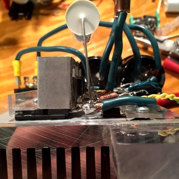
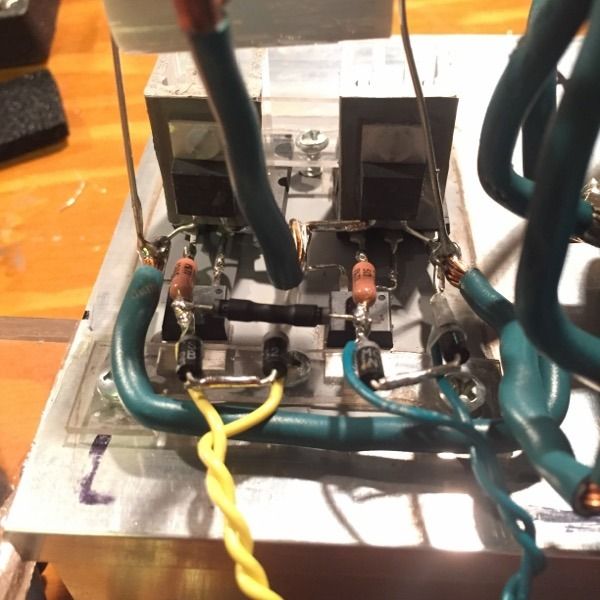
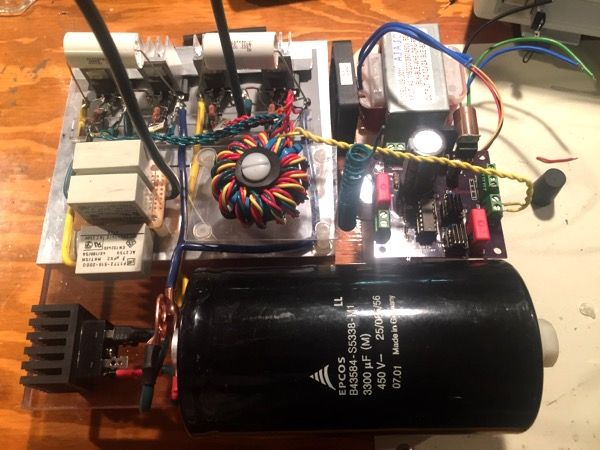
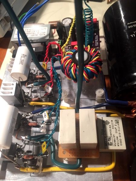
I have had some free time on my hands so I decided why not make an attempt at a full bridge. With left over material and wire I decided to do something more compact.
Well, it's been a tight fit but that's half the fun. Literally.
This coil will run <800w. The coil, w/ a small top load should resonate just under 300kHz.


I used a pentafiliar GDT. It's been phased and tested to be working with an oscilloscope and waveform generator.
Due to lack of space this layout uses a small PC fan but the heatsink is pretty big. I'm hoping that will buy me time as I keep the duty cycles relatively short.

I suppose for ease of mounting I lined up all the MOSFETS in stead of the traditional H configuration.

I have a large 3300uF 450V capacitor just behind the rectifier.
Designing the bridge I have bounced between Kaizer's SSTC II and Steve wards designs


Questions, comments, concerns? Nothing is bolted down yet except for the bridge soldering. The upper deck will be secured with aluminum angle. My male C-14 sockets aren't in yet.
One thing I'm slightly nervous about is the rectifier heat sink is on the small side. I don't have a lot of experience calculating how hot that component will get. No doubler. Should only be seeing standard house main.
Thanks friends.
 
  • Like
Reactions: ped
... full bridge...

...This coil will run <800w....

Lol. Hope you like low coupling or lots and lots of primary turns! Remember, Lpri is the main factor for primary current and thusly Po.


One thing I'm slightly nervous about is the rectifier heat sink is on the small side. I don't have a lot of experience calculating how hot that component will get. No doubler. Should only be seeing standard house main.
Thanks friends.

Measure (or look up) the Vf of the rectifier. Once you've calculated the RMS current desired (from Lpri and F0). Rectifier thermal power waste = Vf * Ipri(rms). Find the thermal resistance of the rectifier and the heatsink on datasheets and find out how many degrees the device will rise in temperature at the waste power figure, if it exceeds maximum temperature you need better cooling or to reduce load. =)

Btw, make sure you fix the phasing error from our email.
 
Last edited:
  • Like
Reactions: ped


Back
Top