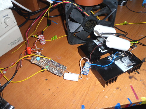
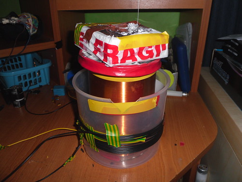
Thanks for the schematic, Sig!
I was able to find the "new" ICs on ebay but I'm not really confident I can pull this off. This is at least some 5 times more complex than any circuit I've ever done

Edit:
After a closer look your circuit isn't much more complicated than his, you just included more detail and the IC "boxes".
I do have some questions:
-What's with the voltage divider between the PWM output and the gate driver's on pins?
-If I got the calculations right you're getting 40kHz to 400 on the PWM, right? Won't I want some lower frequencies for strong interrupted streamers?
-Is that 1:1 transformer really necessary?
-What are all those MUR860's and zeners for?
Sorry for asking too many questions, I'm still learning

The voltage divider drops the 12V output of the PWM chip to 6V which is safe for (most) logiv level inputs. You shouldn't feed 12V in to an input expecting 5V.
I'd have to check the frequency range again, but the frequency set pot and resistor combo are easily modified for different choices. You want >21KHz for audio modulation though, that is a hard-etched requirement, and it sounds much better near 40KHz. SSTCs don't do long arcs, pretty much ever. It just isn't in their nature. With interuption around 130Hz-300Hz you can get slightly longer streamers than would be present in a CW output, but if you just remove the filter capacitors on the DC rails to the bridge and leave it as unfiltered 120Hz pulses from the bridge cap you get a much better power factor, and even longer streamers than with using an interrupter.
The 1:1 transformer is a Gate Drive Transformer (GDT) and is a CRUCIAL part of any inverter technology. It not only isolates the gates from eachother, but also from the logic side of the board, and provides an inverted signal with NO phase errors or delay. In a half bridge the "top" transistor's Source/Emitter will be at positive voltage potential half the time instead of always at ground potential like in a single transistor topology, so if you didn't have a GDT in there you would be putting the positive DC high voltage rail straight in to the low voltage output of your gate drive chips and instantly blow them. The GDT also functions like the primary in a royer oscillator, where placing a pulsing DC positive signal across a coil in different directions produces an AC squarewave which turns what was a DC signal to an AC signal on the secondary of the transformer. This is crucual for multiple reasons, especially as you reach higher frequencies or use transistors with higher gate charges. The Core material for the GDT is VERY IMPORTANT and a bad or incorrect core can destabilize and even destroy the circuit. EasternVoltageResearch sells cores for GDTs which have been specially hand-picked. Also, I can give you the part numbers for the cores that I use from EPCOS if you need. Each secondary winding on the GDT will see the full voltage applied to the high voltage rails of the half bridge and needs to be insulated accordingly. NEVER use bare wire or magnet wire.
The Zeners are for Gate Protection, because we are applying an AC signal to the gates to quickly turn off and remove the charge stored at the transistor's gates. If leakeage or parasitic inductance in the secondary side of the GDT is too high (which is a common condition) the voltage across the gates can spike well over the 20V limit where the gate will die explosively upon applying power to the Drain.
The MUR diodes serve several purposes;
1) The anti-parallel ones across the DS of the fets are called "freewheeling diodes" which removes and blocks the reverse polarity voltage developed by the primary when current stops flowing through it at each half cycle. Without these, that voltage/current is forced to go through the body diode which is either not fast enough to handle it or not robust enough to handle it for long without adding stress to the actual transistor.
2) the series forward biased ones after the MOSFETs' sources are to completely isolate the body diode in order to make it inactive entirely. This migrates heat away from the transistor which will generate its own heat and doesn't need any more. This also doubles the reverse blocking voltage of the transistor further protecting it from killer spikes.
Without these 4 diodes per half-bridge there is about 25% more heating in each MOSFET package, and any sudden stop of current flow to the primary such as when a breaker trips or fuse blows will cause a VERY high voltage Back-EMF (inductive kick) to form across the MOSFETs which will blow them out creating a dead short across both. I've had this happen with even the beefy 500V 100A FDL100N50F's WITH just the anti-parallel MURs on. Adding the series MURs solved the problem. Talk about $4 of diodes saving $50 of MOSFETs.
Looking at his schematic, I understand that the zener diodes are for gate protection; in case the gate drive goes over the zener voltage, the zeners will start to conduct preventing gate damage.
I don't know what the voltage divider is for actually.
The 1:1 transformer on the primary Telsa circuit side is for isolation; it's for safety reasons, and I would recommend keeping it in. It also lets you scope things while the circuit is on without any ground faults causing shorts.
The MUR860 diodes are for protection as well, though I don't think the ones in series with the mosfet's are necessary... the ones in parallel aren't either; the FDL100N50F has an ultrafast diode built into it, so I fail to see the point in them.
That's my take on the schematic anyway!

Pretty good take, see above for diodes and divider.
Thanks for clearing those points! I'm definitely using IRFP260s, those FDL100N50F are way too expensive... but they seem to have the internal diodes as well. Can I safely remove the MURs?
I get the 100N50F's as samples mostly. Remember with the IRFP260s you'll need to limit input AC voltage to the rectifier bridge to less than 120Vac.


