This is an experimental and exploratory thread, not a complete project.
Background:
It is well known to all that there are expensive machines using
super-powerful lasers to cut, drill and etch PCBs in the electronic
industry. It is less known that the new powers provided by extremely
powerful laser diodes accompanied by now accessible high quality lenses,
may provide the some of the same magic to DIY builders.
This project aim to explore the possibility to use laser diodes
to directly etch the copper layer on a PCB.
The main motivation for this project are two videos that appeared a 2
years ago from a user called "Hobby Elektronik". (Who knows, perhaps
he's even a member of LPF?) After those videos there was never any news
or updates about this technology.
(1) PCB Laserprinter (2014-01-04)
(2) PCB Laserprinter Version 2 (2014-02-16)
In the first video it is clear that he only used the laser to etch the
UV mask on the PCB. This is a significant improvement from using regular
UV exposure in terms of speed. Naturally, the next logical step would
be to simply skip the UV and subsequent horrible chemical etching, by
just ablating (etching) the Copper from the PCB directly.
The second video appears to show this, but the comments from the video
maker denies this is the case. However, he has more than a very good
reason to not tell what is really going on. This technology would be a
total game-changer for the hobbyist DIY PCB manufacturer, if viable.
Reading up on the subject, I'm under the impression that this might be
possible. However, I still have not seen any concrete or determinate
results that can confirm or deny this possibility.
I'm hereby reaching out to the LPF community to determine once and for all,
if this is possible using any of our available laser diodes.
No matter what the results, I'd like to find a solution that at least
reproduces or improve upon that solution.
More Video Details:
In the video and accompanying YouTube comments,
we can extract the following info:
CNC paramters:
So here we go, my humble request to the LPF community:
Background:
It is well known to all that there are expensive machines using
super-powerful lasers to cut, drill and etch PCBs in the electronic
industry. It is less known that the new powers provided by extremely
powerful laser diodes accompanied by now accessible high quality lenses,
may provide the some of the same magic to DIY builders.
This project aim to explore the possibility to use laser diodes
to directly etch the copper layer on a PCB.
The main motivation for this project are two videos that appeared a 2
years ago from a user called "Hobby Elektronik". (Who knows, perhaps
he's even a member of LPF?) After those videos there was never any news
or updates about this technology.
(1) PCB Laserprinter (2014-01-04)
(2) PCB Laserprinter Version 2 (2014-02-16)
In the first video it is clear that he only used the laser to etch the
UV mask on the PCB. This is a significant improvement from using regular
UV exposure in terms of speed. Naturally, the next logical step would
be to simply skip the UV and subsequent horrible chemical etching, by
just ablating (etching) the Copper from the PCB directly.
The second video appears to show this, but the comments from the video
maker denies this is the case. However, he has more than a very good
reason to not tell what is really going on. This technology would be a
total game-changer for the hobbyist DIY PCB manufacturer, if viable.
Reading up on the subject, I'm under the impression that this might be
possible. However, I still have not seen any concrete or determinate
results that can confirm or deny this possibility.
I'm hereby reaching out to the LPF community to determine once and for all,
if this is possible using any of our available laser diodes.
No matter what the results, I'd like to find a solution that at least
reproduces or improve upon that solution.
More Video Details:
In the video and accompanying YouTube comments,
we can extract the following info:
Code:
[B]Power Supply/Driver Chipset:[/B]

- Linear Tech, LTC-1446  -- Dual 12-Bit Rail-to-Rail Micropower DACs in SO-8 (for LD reference voltage)
- ??,                    -- Dual Op-Amp for current limiter
- Rohm, BU4053BF         -- Triple 2-Channel Analog Muliplexer/Demultiplexer
- ATmega 88


[B]Laser Head:
[/B]
Laser(s):               2 x 405 nm (to have 2 lines per sweep!?)
Estimated LD Power:     60 - 100 mW
Origin:                 Laserdiode from a XBOX Laser unit
Alignment current:      10 mA
Pulse current:          90 mA
PWM Duty Cycle:         50%
PWM frequency:          60 KHz
Lens:                   AixiZ Blue Laser Glass Lens for 405-455nm
Code:
Speed:                  255 mm/s        (0.18 s/line @ 27.5 mm x 46 mm)
Width:                  0.0508 mm       (with 2227 pixels per 0.0206 mm)
Total Time:             280 s = 3.2 minutes

[B]Laser Modulation:[/B]

start:  50 ms
stop:   50 ms
data:   75 ms
--------------
Total:  ~175 ms/line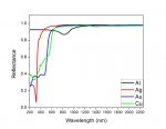
= ~0.18 s/linea) If you are in possession of a high power < 455 nm laser,
please get a one sided PCB and try irradiate it with many different
configurations of:
- LD optical power
- PWM duty cycle
- Lense types
- Focal points
- Cu surface "enhancements" such as heating, abrasion, lacquer,
coloring, and whatever else you can think of...
b) Please document your findings (with pictures) and post them here.
c) Feel free to experiment, but take all safety precautions since polished Cu is highly reflective.
d) Provide any research articles or other documentation of these methods.
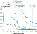
(Cu is one of the most researched elements of the entire Periodic Table!)
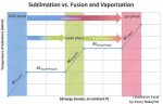
e) It might be useful to get an order of magnitude estimate of how much energy it
takes to vaporize a certain area (spot) of Cu of a standard PCB.
please get a one sided PCB and try irradiate it with many different
configurations of:
- LD optical power
- PWM duty cycle
- Lense types
- Focal points
- Cu surface "enhancements" such as heating, abrasion, lacquer,
coloring, and whatever else you can think of...
b) Please document your findings (with pictures) and post them here.
c) Feel free to experiment, but take all safety precautions since polished Cu is highly reflective.
d) Provide any research articles or other documentation of these methods.
(Cu is one of the most researched elements of the entire Periodic Table!)
e) It might be useful to get an order of magnitude estimate of how much energy it
takes to vaporize a certain area (spot) of Cu of a standard PCB.
Last edited: