Welcome to Laser Pointer Forums - discuss green laser pointers, blue laser pointers, and all types of lasers

Buy Site Supporter Role (remove some ads) | LPF Donations

Links below open in new window

FrozenGate by Avery

Would anyone be willing to give me a couple minutes of help with a circuit?

You misunderstood me. I meant for you to add this as a test to see if it made a difference in the way the MOSFET performed. I understand why you are using it. I'm just trying to troubleshoot this problem with you.


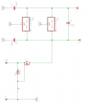
Let me take a different approach to simplify things. Here's a circuit with a simple driver involved. I added two AMC7135 chips to make a basic linear driver (they're helpful because they are so simple that it doesn't add any real question marks to the underlying issue re: using a MOSFET to switch the circuit on).

I also switched to using a P-Channel MOSFET, this one:
http://www.aosmd.com/res/data_sheets/AO3401A.pdf

It can handle 4A, and the AMC7135s will only pull 700mA, so there's no question here about the capacity of the MOSFET to handle the current.

attachment.php


What do you think? Electronically sound? This should work?
 

Attachments

  • example.png
    example.png
    11.8 KB · Views: 175
Yeah, the AMC1735s are constant current sources at 350mA each. You have two in parallel so that should give you the 700mA you are looking for. The change to a P channel enhanced MOSFET looks okay, so I see nothing here that should cause you any foreseeable problems. The quiescent current of the current regulators is very low, so unloaded they won't even be part of your circuit. Are you planning on using this to drive a S06J sled 405nm laser diode? Seems like a good driver for that purpose. Let me know how it turns out.
 
Yeah, the AMC1735s are constant current sources at 350mA each. You have two in parallel so that should give you the 700mA you are looking for. The change to a P channel enhanced MOSFET looks okay, so I see nothing here that should cause you any foreseeable problems. The quiescent current of the current regulators is very low, so unloaded they won't even be part of your circuit. Are you planning on using this to drive a S06J sled 405nm laser diode? Seems like a good driver for that purpose. Let me know how it turns out.

I probably won't actually make the AMC7135 circuit in my previous post, it was just an easier way to illustrate the MOSFET implementation than leaving the driver empty.

I'm still struggling to grasp why my previous circuit burned up. Oh well.
 
I still think it was your load, but not having the thing in front of me I can only speculate. I can't think of anything else it could be.
 
RHD,

You've got to get your gate voltage, and load current on a scope to check things out.

Even something like a cheap switch that "switches" poorly can allow sloppy and damaging di/dt into the gate.

Do you have a picture of your setup?

My first guess could be that there is possible (but not necessarily probable) damage to the gate during the turn on transient. Try adding a 100 ohm resistor in series with the gate.

The circuit you copied demonstrates well, the voltages that need to be present for a small, basic switched load. But it does not take into account other physical processes that can take place when your load is more complicated.

For instance, a (cheap) switching circuit is more likely to have noise - everywhere on it. Even on its 'GND" terminal - especially if there is a poor connection from the circuit to GND. Its GND node could be sitting at an unstable voltage directly affected by the switching noise. Let's say this is happening - severely. One could add a bypass capacitor across the drain and the source in an attempt to make the load look more like a smooth and stable DC load with no AC quirks about it.

But that is just one example. If a switching circuit is killing things off, there could be some inductive feedback getting back to your FETs drain somehow.. it would depend on the topology of the switching circuit of course.

For now, try adding a series resistor on the gate, a rectifying diode in series with your load and the drain, and a capacitor in parallel with your FET. Just see what happens. Sometimes you just have to continue with additional experiments.

Honestly though, I would be surprised if that helps at all. I'll go back to what I said initially. What would help most quickly is a nice set of startup and shutdown transients, as well as some steady state current measurements all about if possible. Some pictures of your experimental setup is also a bonus. :)
 
Thanks Meatball, that's really helpful. What I may start with is the 100 ohm resistor on the gate.

A diode in series with the load would drop voltage, so I want to avoid that.

Each iteration takes about a month (Oshpark to Canada is slow).

There's not much to show re setup. It's just a small pcb.
 
Hmm. Referring to a noisey gate switch as the derivative of the gate current with respect to time is a novel way of expressing random noise and is something I had to do a double take to believe I actually read that. That would indeed have to be an exceptionally noisey switch to cause the damage that's been described. And that inductive reactance in the drain circuit would be more likely part of the load. A scope would be helpful. I have one, but most members of the forum don't, so I don't see rhd going that route. And hanging caps between the source and drain, wouldn't a filter cap off the drain to ground be just as, if not more, effective? I don't know, maybe I'm just getting too old. lol
 
I did notice you have a schottky diode across the low side of the LD and ground.

Wrong. That is a zener, and this is inherent in mosfet design - it cannot be removed from the circuit.

all the power dissipated through your driver will go through your MOSFET. You may want to check the power dissipation of your entire circuit and see if your MOSFET can handle it

Wrong. The power that is dissipated in the driver is dissipated ONLY IN THE DRIVER. Heat does not teleport. The power dissipated in the FET will be the drain current squared multiplied by the RdsON value.

rhd, it occurred to me that if you are trying to push all your power through this MOSFET you might be better off by using a DMOS instead of a CMOS FET.

Wrong. This is a discrete N-MOS part. The C in CMOS stands for complimentary, which means there is both NMOS and PMOS on a circuit.


rhd, your problem is likely a combination of driving the gate properly, and selection of a FET with very little headroom. I'd get a bigger FET and put a 100R on the gate.
 
Last edited:
Wrong. That is a zener, and this is inherent in mosfet design - it cannot be removed from the circuit.


Wrong. The power that is dissipated in the driver is dissipated ONLY IN THE DRIVER. Heat does not teleport. The power dissipated in the FET will be the drain current multiplied by the RdsON value.


Wrong. This is a discrete N-MOS part. The C in CMOS stands for complimentary, which means there is both NMOS and PMOS on a circuit.


rhd, your problem is likely a combination of driving the gate properly, and selection of a FET with very little headroom. I'd get a bigger FET and put a 100R on the gate.


You are right. I misspoke when I said the power was dissipated through the MOSFET, it is dissipated mostly in the driver , what I meant to say was the current would pass through the MOSFET. Also, CMOS was an unfortunate use of the term because as you pointed out it is the combination of a P MOS and N MOS that make up a CMOS. The diode incorporated in the MOSFET could indeed be a zener I didn't have a good look at it and the two are similar in appearance when the picture is unclear. Sorry for the mistakes. It was late when I first got involved in this circuit and I was doing several things at once the next day. BTW, won't the power dissipated in the FET be Id^2 X RdsON? The drain current x RdsON= Vds
 
Last edited:
Wrong. The power that is dissipated in the driver is dissipated ONLY IN THE DRIVER. Heat does not teleport. The power dissipated in the FET will be the drain current multiplied by the RdsON value.

Wrong. the power dissipated in the FET is Id^2 X RdsON. I left the thermal part out because this is in saturation and it doesn't matter that much. Drain current multiplied by RdsON=Vds which in saturation is pretty low unless the temperature rises dramatically.


rhd, your problem is likely a combination of driving the gate properly, and selection of a FET with very little headroom. I'd get a bigger FET and put a 100R on the gate.[/QUOTE]
 
rhd, your problem is likely a combination of driving the gate properly, and selection of a FET with very little headroom. I'd get a bigger FET and put a 100R on the gate.

Thanks Cyparagon. That is essentially the conclusion I came to - or at least the approach to testing I decided to take in my next iteration.

It was really frustrating that a circuit that shouldn't be problematic, was.
 
Did you try a different temporary load? your driver may have large value ceramic caps at the input which have very low ESR which can blow mosfets with the inrush current at startup.

You can also try to power the driver directly off the battery just to make sure it is working right just to rule it out.
 
Cyparagon, I noticed you changed your "mistake" after I brought it to your attention. Yes, I did misspeak on a couple of things, but I tried to explain what I said an what I meant. You didn't post my earlier description of the diode being part of the MOSFET, you simply quoted a mistake in wording on my part in a later post. And now I find that you have tried to screw with my reputation after doing that. Well, you were very WRONG in your explanation of the power dissipation in the MOSFET as being the drain current multiplied by the RdsON. You simply changed the post after I brought it to your attention. Everyone makes mistakes in what they are trying to convey from time to time, even you. And stating that I was talking about something that I didn't know anything about is just bad manners. You don't know me and I didn't start this pissing fight, but if that's what you want, then bring it.
 
You don't know me and I didn't start this pissing fight, but if that's what you want, then bring it.

No. No "bringing" of anything. No fighting. Everyone here was just trying to help, which is the right spirit for this forum.

It's okay to get things wrong. If I hadn't gotten something wrong in the first place, this thread wouldn't be here.

Let's stay on track. I'll keep everyone updated on my next iteration's success / failure.
 
Last edited:
What was the MOSFET connected to during the test? What I mean is was it soldered to a board, or
connected to alligator clips, or soldered to wires? The 60-100mW of heat has to get out of the chip
somehow. Usually on these small surface mount parts it goes through the leads into the copper pads
on the circuit board. Take a look at the suggested pad layout on the datasheet. Your pads have to be
at least that size to sink away the heat. Alligator clips or sockets will cause all kinds of problems.
These small chips really have to be soldered to a board for testing. You may also get away with
soldering to wires, but they have to be a heavy enough gauge and it has to be done right.

The other thing to be concerned with is ESD. MOSFETs are not as bad as LASER diodes when it
comes to ESD, but they are a close second. I have blown MOSFETs by improper handling before. It
causes all kinds of funny problems.

I also agree with the other guys about the switch bounce being a possible problem. The pull-down
resistor should be more like 10k, or else the gate is going to discharge slowly through the linear region
and possibly cause problems, especially during a bounce condition. You want as quick and clean of a
low-high-low transition as you can get. Otherwise, I see no reason why this transistor should not work.
rkcstr was using something similar on his driver.
 
Last edited:


Back
Top