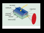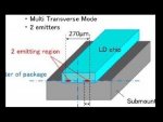

Ok the top pic is what we have in a single beam diode and the 2nd pic is the 2 beam mitsu, the space between the 2 active regions is just missing dopant IINM so what we see when we look at 2 spreading beams is really one very wide beam with the center missing, it's the curvature of our lens and the divergence that makes the 2 beams spread so typical beam shaping should bring the 2 beams into line such as using a c-lens pair or FAC lens.
If there were 2 chips inside the diode then we could see them aligned to match a lens and a task, but as this is 2 emitting regions in the same chip it's basically a wide beam missing it's center.
So just as a C-lens pair will reduce the divergence after the primary collimating lens the same pair would reduce the spread of the 2 beams as they are the outer portions of basically a very wide beam missing it's center, this could be a good place for a FAC lens just in front of the diode can window before the primary collimating lens to produce 2 close to parallel beams.


----------------------
On to that osram PLPT9 450C
I wonder if that osram 3.5 is basically a NDB7A75 possibly with slightly better divergence ?
I have some 7A75's in a big heat sinks @ 4.0a with a G3 and 3.3x BE and they are not bad, if the divergence was like a 7875 but could do 5w like 7a75 that would be nice, but I somehow don't expect divergence to be that good, fingers crossed....but it's _E as in experimental so we may not see much of it, still never saw that 20 emitter 25 x 32 mm micro block


