Just discovered a fantastic article in the April issue of SciAm, talking about work on creating GREEN laser diodes!!! 
The article also has some good info on the invention (and inner workings) of cost-effective Blu-Ray diodes, which was apparently created by the same folks who are now developing blue and green! (Good stuff to know, may shed some light on the peculiarities of the PHR-803T diodes?)
pullbangdead, I know you mentioned you have access to some nice meters, but why didn't you tell us you guys were having so much fun out there at UCSB!
Some key highlights -
The same technological breakthroughs at UCSB that allowed the creation of low-cost high-yield Blue-Ray (actually violet) laser diodes, are now being extended to develop blue and green laser diodes!
Indium - use of an ultra-thin (nanometer-scale) active layer of Indium Gallium Nitride between N and P-doped Gallium Nitride layers, to form a "quantum well".
Growing the diodes on a pure crystalline Gallium Nitride substrate (base), rather than traditional Sapphire. Apparently growing these on top of Sapphire produces a lot of submicroscopic crystalline defects / irregularities, which can propagate upwards through successive layers as the diode is grown. These defects act as centers where electrons and holes recombine to produce undesirable heat, rather than light. Interesting quote -
Reportedly, the lasers used in Blu-Ray players and PS3 are grown on top of sapphire, which as substrates go, is relatively cheap and widely available. I cannot help but wonder if the # of these defects in a particular LD could be the cause of the wide variance in efficiency and output levels being reported here in individual Blu-ray diodes?
Using a pure Gallium Nitride substrate results in far fewer of these mismatch defects, and can thus produce much more laser light, with a lot less heat!
By adjusting the amount of Indium in that thin active layer, you can also alter the wavelength of the laser light produced! Key concept here -
Of course, nothing is ever that simple - there are a few difficulties standing in your way!
First off, the crystalline structure of the Gallium Nitride apparently creates strong electrostatic fields which tend to drive the electrons and holes away from each other, fighting against the applied current, and making it more difficult for them to combine to create light. This "quantum-confined Stark effect" also becomes a much greater problem when you try to shift the wavelength from violet to blue to green.
Even worse, the amount of current/energy required to overcome this effect at the longer wavelengths (like green) results in the electrons & holes combining at higher energy levels, shifting the generated light's wavelength back towards violet!
This is reportedly the main reason why we don't have green LDs.
Another major problem is that Indium Gallium Nitride must be grown at much lower temperatures (700C) than the surrounding Gallium Nitride layers (1,000C), as the higher temps cause the Indium to disassociate from the material!
So when you then try to grow the Gallium Nitride layer on top, the extra heat can cause the Indium in the layer below to form "islands" of inhomogeneous indium alloys, which causes the electron-hole recombination energy levels to vary from one place to another, resulting in different wavelengths of light being generated and a broad emission spectrum - OK for making LED's, but not so good when you are trying to produce monochromatic light for a laser!
Because higher amounts of Indium are needed to produce longer-wavelength light, this Indium island problem becomes more severe when trying to create blue and especially green laser diodes.
But the good boys at UCSB are riding to the rescue! [smiley=thumbsup.gif]
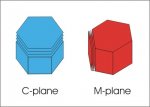
On the seemingly insurmountable electrostatic effects which have reportedly prevented the creation of a green LD for over a decade, they realized that this was a result of the crystalline structure of the traditionally-cut "C-plane" (horizontally sliced like a stack of pancakes) Gallium Nitride crystal, and that by cutting the crystal along the "M-plane" (vertical slices from one of the facets on the side of the crystal, see my funky Corel graphic below) instead, they could solve this problem!
Of course, finding pure Gallium Nitride wafers sliced this way was a bit of a problem. : But in 2006 Mitsubishi started providing small ones (~1cm) of the required quality to UCSB. On Jan. 27, 2007, a UCSB graduate student created the first working nonpolar GaN laser diode using one of these wafers, generating a blue-violet beam at a wavelength of 405nm! (hmm, sound familiar?)
On the Indium "island" problem, a solution was also forthcoming.
In order to overcome the aforementioned electrostatic problem, Blu-Ray LD manufacturers had been creating extremely thin Indium Gallium Nitride layers (under 4nm, or only about 20 atoms thick!), in order to keep the electrons & holes bunched closer together, maximizing the chances they could combine and create light.
But by solving the electrostatic issue, thicker active layers can now be used (up to 20nm). And while Indium islands would still form, they tend to be confined near the layer boundaries, leaving the center area of this thicker active layer free to create monochromatic laser light!
The article goes into much greater detail on this and other things, but by using all of this magic, they have been able to achieve some pretty amazing results!
This has included -
A blue-violet LED with an efficiency > 45%!
A blue-green Laser Diode, running at 481nm!
An optically-pumped (rather than electrically) Laser Diode, producing 514nm (green) laser light!!!
How cool is that!
On a side-note - I guess I must be learning something here at LPF, because I actually caught the esteemed Scientific American magazine making several laser-related technical errors in a side-bar to this article about green laser pointers! -
Hmmm...what could possibly be wrong with that description? :
So I sent them a correction!
The print magazine has cool graphics & lots of extra info and is definitely recommended, but as it's the current issue, the basic article is also available online here -
http://www.sciam.com/article.cfm?id=dawn-of-miniature-green-lasers
Enjoy!
my funky Corel graphic -
The article also has some good info on the invention (and inner workings) of cost-effective Blu-Ray diodes, which was apparently created by the same folks who are now developing blue and green! (Good stuff to know, may shed some light on the peculiarities of the PHR-803T diodes?)
pullbangdead, I know you mentioned you have access to some nice meters, but why didn't you tell us you guys were having so much fun out there at UCSB!
Some key highlights -
The same technological breakthroughs at UCSB that allowed the creation of low-cost high-yield Blue-Ray (actually violet) laser diodes, are now being extended to develop blue and green laser diodes!
Indium - use of an ultra-thin (nanometer-scale) active layer of Indium Gallium Nitride between N and P-doped Gallium Nitride layers, to form a "quantum well".
Growing the diodes on a pure crystalline Gallium Nitride substrate (base), rather than traditional Sapphire. Apparently growing these on top of Sapphire produces a lot of submicroscopic crystalline defects / irregularities, which can propagate upwards through successive layers as the diode is grown. These defects act as centers where electrons and holes recombine to produce undesirable heat, rather than light. Interesting quote -
The presence of these defects played havoc with production yields when Nichia and Sony first tried to manufacture blue laser diodes.
Reportedly, the lasers used in Blu-Ray players and PS3 are grown on top of sapphire, which as substrates go, is relatively cheap and widely available. I cannot help but wonder if the # of these defects in a particular LD could be the cause of the wide variance in efficiency and output levels being reported here in individual Blu-ray diodes?
Using a pure Gallium Nitride substrate results in far fewer of these mismatch defects, and can thus produce much more laser light, with a lot less heat!
By adjusting the amount of Indium in that thin active layer, you can also alter the wavelength of the laser light produced! Key concept here -
By increasing the indium concentration in the alloy, one can lower this energy, thereby increasing the wavelength of the light and changing its color from violet to blue to green.
Of course, nothing is ever that simple - there are a few difficulties standing in your way!
First off, the crystalline structure of the Gallium Nitride apparently creates strong electrostatic fields which tend to drive the electrons and holes away from each other, fighting against the applied current, and making it more difficult for them to combine to create light. This "quantum-confined Stark effect" also becomes a much greater problem when you try to shift the wavelength from violet to blue to green.
Even worse, the amount of current/energy required to overcome this effect at the longer wavelengths (like green) results in the electrons & holes combining at higher energy levels, shifting the generated light's wavelength back towards violet!
This is reportedly the main reason why we don't have green LDs.
Another major problem is that Indium Gallium Nitride must be grown at much lower temperatures (700C) than the surrounding Gallium Nitride layers (1,000C), as the higher temps cause the Indium to disassociate from the material!
So when you then try to grow the Gallium Nitride layer on top, the extra heat can cause the Indium in the layer below to form "islands" of inhomogeneous indium alloys, which causes the electron-hole recombination energy levels to vary from one place to another, resulting in different wavelengths of light being generated and a broad emission spectrum - OK for making LED's, but not so good when you are trying to produce monochromatic light for a laser!
Because higher amounts of Indium are needed to produce longer-wavelength light, this Indium island problem becomes more severe when trying to create blue and especially green laser diodes.
But the good boys at UCSB are riding to the rescue! [smiley=thumbsup.gif]
On the seemingly insurmountable electrostatic effects which have reportedly prevented the creation of a green LD for over a decade, they realized that this was a result of the crystalline structure of the traditionally-cut "C-plane" (horizontally sliced like a stack of pancakes) Gallium Nitride crystal, and that by cutting the crystal along the "M-plane" (vertical slices from one of the facets on the side of the crystal, see my funky Corel graphic below) instead, they could solve this problem!
Of course, finding pure Gallium Nitride wafers sliced this way was a bit of a problem. :
But in 2006 Mitsubishi started providing small ones (~1cm) of the required quality to UCSB. On Jan. 27, 2007, a UCSB graduate student created the first working nonpolar GaN laser diode using one of these wafers, generating a blue-violet beam at a wavelength of 405nm! (hmm, sound familiar?)On the Indium "island" problem, a solution was also forthcoming.
In order to overcome the aforementioned electrostatic problem, Blu-Ray LD manufacturers had been creating extremely thin Indium Gallium Nitride layers (under 4nm, or only about 20 atoms thick!
), in order to keep the electrons & holes bunched closer together, maximizing the chances they could combine and create light. But by solving the electrostatic issue, thicker active layers can now be used (up to 20nm). And while Indium islands would still form, they tend to be confined near the layer boundaries, leaving the center area of this thicker active layer free to create monochromatic laser light!
The article goes into much greater detail on this and other things, but by using all of this magic, they have been able to achieve some pretty amazing results!
This has included -
A blue-violet LED with an efficiency > 45%!
A blue-green Laser Diode, running at 481nm!
An optically-pumped (rather than electrically) Laser Diode, producing 514nm (green) laser light!!!
How cool is that!
On a side-note - I guess I must be learning something here at LPF,
because I actually caught the esteemed Scientific American magazine making several laser-related technical errors in a side-bar to this article about green laser pointers! -WHAT ABOUT GREEN LASER POINTERS?
The green lasers that have long been available employ a complicated two-step process...Semiconductor lasers inside these devices emit infrared radiation with a wavelength around 1,060 nanometers. This radiation then pumps a crystal that oscillates at half this wavelength - about 540 nanometers...the second crystal can heat up, altering the wavelength...
Hmmm...what could possibly be wrong with that description? :
So I sent them a correction!
The print magazine has cool graphics & lots of extra info and is definitely recommended, but as it's the current issue, the basic article is also available online here -
http://www.sciam.com/article.cfm?id=dawn-of-miniature-green-lasers
Enjoy!
my funky Corel graphic -