Welcome to Laser Pointer Forums - discuss green laser pointers, blue laser pointers, and all types of lasers

LPF Donation via Stripe | LPF Donation - Other Methods

Links below open in new window

ArcticMyst Security by Avery

Eagle PCB design software help!

Fiddy

0
Joined
May 22, 2011
Messages
2,726
Points
63
G'day,

A question for someone in the know,

Im making my first PCB and im pretty much done but ive found what i think is a problem.

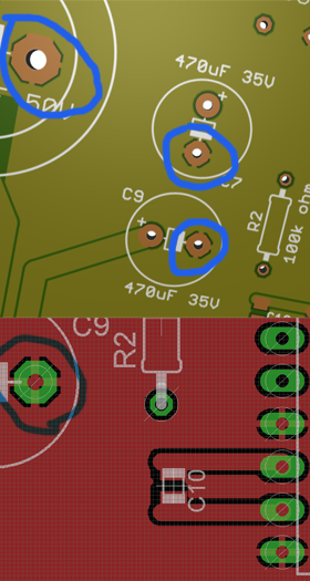
ive got a big polygon on each side of the board (GND is top ,12V+ is bottom) and when i connect pins to the polygon i get this cross-hair looking connection to the polygon, see this photo:

polygonconnections_zpsaa0df7b4.png


Is that normal to send of to get the boards made?

if not, how to i get a better connection like with other connections that arnt to a polygon?

Cheers! Fiddy.


Things

0
Joined
May 1, 2007
Messages
7,517
Points
0
Hey mate, replied to your PM :)

For anyone else wondering, it's a technique called "thermal relief", it makes soldering to the pads a crapload easier because all the heat isn't sinked away to the copper as fast :)
 
Joined
Feb 1, 2008
Messages
2,894
Points
0
Its about as good as any other trace to pad connection, except there are 4 connections there, not just 1. So, it should technically be better. :)
 
Joined
Oct 26, 2007
Messages
5,438
Points
83
Equally important, whatever you solder to that pad/hole has a solid connection, rather than a cold joint, or damage from overheating.
 
Last edited:

Things

0
Joined
May 1, 2007
Messages
7,517
Points
0
If it's for a very high current thing, like a tesla coil, I'd recommend at least thickening them a bit so they don't become instant fuses when you discharge the caps, but apart from that, should be fine. A general rule of thumb is allow 10mil of trace for 1A for 10C rise :)
 

Fiddy

0
Joined
May 22, 2011
Messages
2,726
Points
63
If it's for a very high current thing, like a tesla coil, I'd recommend at least thickening them a bit so they don't become instant fuses when you discharge the caps, but apart from that, should be fine. A general rule of thumb is allow 10mil of trace for 1A for 10C rise :)

Yeah it is actually, ive redone that guys plasma speaker board :D

Ill have to find out to make the copper pour connection take up all of the pad or make the 4 small connections on the pad bigger, i saw benmvw do it on his benboost:

36482d1328852762-free-diy-open-source-boost-driver-tested-working-ld-boost-driver-lm3410-r6-fork-again-r9-back-.png
 
Last edited:

benmwv

0
Joined
Sep 10, 2010
Messages
1,380
Points
48
Hey replied to your PM but ill say it again here for anybody else.

To make them solid in eagle go in design rules and on one of the last tabs (second to last I think) change thermal isolation to 0.

I've never had any problems with it being hard to solder and I like to keep all my connection solid. Especially when you have a surface mount part in dpack or something. It wont connect the tab to the ground plane except for 4 tiny connections. You definitely don't want your hot parts thermally isolated like that.
 

canan

0
Joined
Aug 29, 2013
Messages
1
Points
0
Hi, thanks for the info @benmwv. I was going through this thread and I still have one little question, this is just a normal trace, the polygon. Essentially it’s nothing different than the other traces on the board except for its shape which isn't perfectly round. Theoretically speaking, how does it work? I searched on google and found out that thermal relief means connecting a PCB to a copper pour using a thermal connection which essentially is just spooks of copper connecting it to the surrounding board. I'd be thankful if you can explain this a little more. Thanks for the info anyways.
 
Last edited:


Top