Welcome to Laser Pointer Forums - discuss green laser pointers, blue laser pointers, and all types of lasers

LPF Donation via Stripe | LPF Donation - Other Methods

Links below open in new window

ArcticMyst Security by Avery

TPS63020 Based Driver

HTV

0
Joined
Sep 21, 2011
Messages
18
Points
0
This is written by author our scheme with TPS 63020. His nick is INFERION. He don’t speak English.


Hello rfhv,


I noticed your scheme, it looks a lot like mine. Your scheme has a difference in current sensor in essence. I tormented this chip long time ago. I think, the cause of ripple is in very sensitive feedback of TPS, not in slower INA138. This is general problem for all chips of this line. FB pin is intended only for active linear load such as resistor. Steep volt current characteristic increases error signal by a factor of ten that is a cause of overcorrection. This is a cause of unstable work of chip. Decreasing the ripples isn’t easy task. So, I dropped this scheme. You can solve this problem by increasing of output capacity, but I don't like the final result in this case. I can make more powerful driver in this dimensions, for example on STM32…

I see a familiar picture on your oscillograms. This is a sing at 200 KHz. It is much lower than work frequency of TPS. Feedback is singing, scheme excites itself. Low efficiency and large heatsink on previous pictures alert. My scheme “worked” too, but very heated and I saw same pictures on my oscillograph. Also, if I load my driver by resistor, then it works well.

You think that there isn’t something terrible in ripple at 200 KHz, but it is a tips for unstable work of TPS. Results of it work in this mode will be unpredictable.
 
Last edited:


Joined
Mar 29, 2011
Messages
1,056
Points
48
I think I just saw an error in your layout.

The VIna which is connected to the cap 100nF to ground.

BUT!!!

You have it connected to the POWER GROUND.
You don't have a separate island for the CONTROL GROUND. There must be a control ground node connected as close as possible to pin 2 separated from the Power/Common Ground.

You can connect pin 2 to the common ground under the IC(as you probably did) but you a need a separate island for control logic. The VIna cap MUST be connected to it and the feedback resistors MUST be connected to it!
 
Last edited:

rfhv

0
Joined
Nov 17, 2011
Messages
14
Points
0
Yes, I just used a single ground. I think split grounds are a bit overrated.

In any case, I got the driver stable. I was able to remove all the ripple from the output with the addition of a capacitor and a resistor.

The Russian suggestion was correct. All I needed to do was limit the high frequency gain of the feedback loop.

More details to follow...


EDIT: At 3.73 V in, 1.80 A out, I achieved 84.4% efficiency. Ripple is 10 mA max at greater than 2.4 Mhz. The ripple is just switching noise at this point.
 
Last edited:
Joined
Aug 8, 2010
Messages
4
Points
0
Hello guys, it isn’t my first post on your forum, but it is the first one that was posted by myself. I see you discuss my schemes. So, I decide to register at this forum and join to your community. Sorry for my English, I didn’t speak English well. All my messages will be duplicated in my native language under spoiler just in case.

I’ll tried to build different variants of this scheme more that year ago. I tried different layouts too. Connect instead of LD resistor at 3..5 Ohm. Will oscillation disappear? My driver worked stable in this moment. Cause is in hard voltage-current characteristic of 445 LD.

I can suggest 3 version of solution for it problem.

The first solution
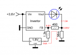
1.PNG
Feedback is decoupled for AC and DC. Signal of error comes from TPS out directly, therefore Feedback works in standard mode for voltage regulator (capacitors are potential divider). And voltage was regulated for LD'a current at the expense of displacement. I don’t see any preferences of this variant, only imperfections. First, feedback is very slow. Second, it can work stable in narrow voltage range because signal is constant and isn’t depend of input voltage (it depends of current-voltage characteristic’s slope).

The second solution
2.PNG
It’s same story under different view. Capacitors were substitute for resistor with power supply. Resistor is something like CV generator. Also, it adds 0.45V to signal from current shunt . So, signal of error (and shunt's voltage dip with it) is suppressed in 10 times. Performance of feedback isn’t slower than typical, signal of error isn’t snapped to out voltage and now.

The third solution
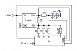
3.PNG
It’s monster with microcontroller. I tried to gather couple of variants and was disappointed by DAC both times. Third times I gathered set of resistors that have to replace DAC (as at a scheme), but I invented more interest thing in this time. Since that time, I don’t work at driver with TPS63020.

How can I hide a text under spoiler?

P.S. I am not Russian. I am Ukrainian :).
 
Last edited:

rfhv

0
Joined
Nov 17, 2011
Messages
14
Points
0
Here is the driver with the ripple removed. Ripple is less than 10 mA at 2.4 MHz. The scope shots are 10 mA per division. Coupling is AC, probe is 10X.

The bench meter shows output current. The green meter in the center shows the voltage across the load. The power supply is putting out 4 V which drops to about 3.7 V at the laser driver due to the resistance of the wires. The scope shows the current through the test load.

Here I am doing 2 A into my test load.
laserdrive_rev3_A.jpg


And here is 1.8 A into the test load.
laserdrive_rev3_B.jpg


Here is a scope shot of the ripple.
laserdrive_rev3_C.jpg


Here is what I built.
laserdrive_rev3_sch.png
 
Joined
Aug 8, 2010
Messages
4
Points
0
How did you chosen C9 capacitance? Too big will resulted inrush current at startup, but too small causes amplitude and phase distortions of the signal. In first event solution may be easy, but second makes my face pensive.
 
Last edited:

rfhv

0
Joined
Nov 17, 2011
Messages
14
Points
0
I experimented to find the value of C9. I do have some overshoot at startup. I get a spike of about 2 A that lasts for less than 1 ms. I do not expect this to be a problem for the 445nm diodes that everyone uses but if you wanted to use this for a 405 nm diode for example, you should probably choose a different driver.

This is just as well to me, as the flex drive already fills the need for a low current driver. I intend this product to be used mainly for diodes that require 1.5 A and up.

From your previous post I tried a modified version of solution 1 that you proposed. This arrangement proved to be less stable than the arrangement I am currently using. I intend to tweak the values of your proposed solution 1 at some point and see if I can get the driver to be stable and overshoot free.
 
Joined
Dec 27, 2011
Messages
2,062
Points
48
This is an interesting thread that just sort of petered out. I'd love to hear back from inferion about the circuit and what he thinks of the final version. It sounds like that if there were a way to tame the over current on startup, that it would be a decent driver.
 
Last edited:
Joined
Aug 8, 2010
Messages
4
Points
0
I suggested upstairs in this thread solutions of this problem. The first one is very simple; we need to add to current scheme only one capacitor. But, it looks like nobody did it. I have more interesting projects that I want to complete. I had interest to TPS63020 in past, but I lost it after some failures. Now, I know that can be done, but I haven’t interest to it. Maybe, I’ll back to this scheme in future, if this thread will be actual. I don’t see perspectives of this driver. It is expensive. I can make more powerful and cheaper diver using some microprocessor.


Top