Welcome to Laser Pointer Forums - discuss green laser pointers, blue laser pointers, and all types of lasers

Buy Site Supporter Role (remove some ads) | LPF Donations

Links below open in new window

schematic simplification.

Joined
Jun 27, 2011
Messages
79
Points
8
I have a schematic for a circuit and the ic's pins are reordered (as usual) but this is a rather large circuit so I would like it to be as simple as possible. Is there any software that can be used to do this or any tip you guys can give me?

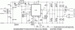
Attached is the schematic i am trying to simplify. Just saying, this is not my work at all and am not taking credit for any part of its design.
 

Attachments

  • sstc01.gif
    sstc01.gif
    21.6 KB · Views: 3,074
Last edited:


That circuit looks simple enough...
The designer of the circuit surely did not add
extra parts just to make it look pretty..

Parts are added to circuits for a reason....


Jerry
 
Last edited:
I didnt say he added anything for no reason. I realise how you interpreted what I said as that though. what I meant was is there an easy way to redraw that circuit with the ic's pins in order (like on the physical component) I know how to do it but it wont necessarily be the neatest possible way. i just didnt want wires everywhere all over the back of the circuit board I create, I would prefer tracks.
 
I assume you are building the circuit point to point
by hand.
You can make a copy of the Schematic and use a
yellow marker to trace each line that you actually
wire to your physical circuit.
That's what we do in the shop on special projects
to not miss a connection or trace.

The only other way I could see would be to re-draw
it by hand...


Jerry
 
Redrawing it by hand may not be a bad idea - gives you a sense of where the components actually go when you want to build it on protoboard or something like that.

I'm curious how it connects to the gates of mosfets though, especially the A and D outputs that seem to be DC isolated.
 
So you've got an SOIC adapter board for this chip? The main reason it's drawn up that way is because the chip will more than likely be used in an auto-routed PCB anyway; the understandable circuit representation is more useful for most designers.

I'd go with what Benm said and just redraw it by hand, because more than likely you won't find a chip-drawn version anywhere else.
 
Thanks guys. Ill just redraw it. Ohh and benm the outputs (A+B and C+D) are inputs for 2 gate driver tansformers with 2 secondarys and one primary. Would post scematic but I'm on an iPhone amd cbf. From my understanding this isolates the 240v side from the control side. It's richie burnetts design, just google him.


Back
Top