

JLSE
1
- Joined
- Dec 13, 2007
- Messages
- 3,580
- Points
- 0
I recently started etching my own boards in practice to get up to the ability to etch SMT layouts. I have had a decent ammount of sucess in that the boards I make are a little bit better and smaller each time around. I use the 'toner transfer method', ironing the print onto the copper clad.
The problem I have run into is scaling it down. I am using a program called 'express pcb', one of the major problems ive been having is that I cant paste the final design into photoshop or MS Word. It says copy to the clipboard, but only pastes blank white or black squares, no board traces No matter what I have tried, it just wont work. I have had to screen shot the layout and trace the jpeg out in photoshop
I am looking for a non-trial program that will work with less headaches, if any of you guys know of a good app for this, please post a link.
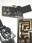
Here is my first off, of a Jr. LM317. You can see the board was taken out of its vibrating acid bath a bit too early, and was more or less just a test to ensure it all worked. This is so far the smallest I have made, it fits nicely into an axiz module, and is great for lower power diodes.
Any ideas?
Thanks in advance,
Joe.
The problem I have run into is scaling it down. I am using a program called 'express pcb', one of the major problems ive been having is that I cant paste the final design into photoshop or MS Word. It says copy to the clipboard, but only pastes blank white or black squares, no board traces
No matter what I have tried, it just wont work. I have had to screen shot the layout and trace the jpeg out in photoshop I am looking for a non-trial program that will work with less headaches, if any of you guys know of a good app for this, please post a link.
Here is my first off, of a Jr. LM317. You can see the board was taken out of its vibrating acid bath a bit too early, and was more or less just a test to ensure it all worked. This is so far the smallest I have made, it fits nicely into an axiz module, and is great for lower power diodes.
Any ideas?
Thanks in advance,
Joe.


")
")