HIMNL9
0
- Joined
- May 26, 2009
- Messages
- 5,318
- Points
- 0
^ Probably, instability due to bad pcb or resonance ..... i made some trials, with 3410, and i can say you something, but i'm not a 3410 expert, nor an NS engineer  , so, take them for that what they can worth.
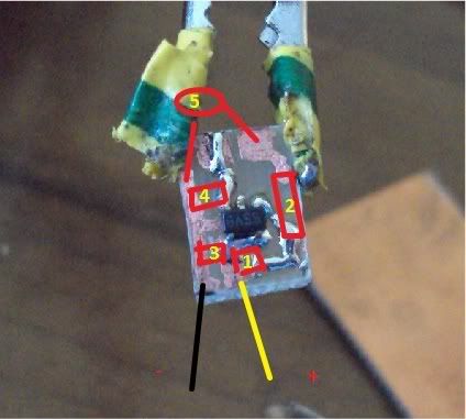
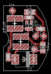
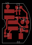
First, as also IgorT said you, you need at least 10uF electrolitic tantalium, or 22uF standard electrolitic capacitor at the input, better if paralleled with a 220 or 470 nF ceramic capacitor ..... second, draw the pcb carefully, trying to keep all the connections the shortest possibles, especially the ones related to the coil and schottky diode, and the grounds ..... also, be abundant with the ground pads for heat dissipation ..... third, try to not put capacitors from the pin 1 (in your package is the switching pin) and the ground, but only from the positive output and the ground (i mean, from after the switching diode, and the ground pad), and also here, you need probably a good capacitor value ..... i was using 47uf tantalium paralleled with 1uf ceramic, at the output.
Also, don't place capacitors from the pin 3 and ground (practically, in parallel to the current sensing resistor), if you want a fast response current regulation ..... probably, you can place a 100nF capacitor there, but no electrolitics ..... anyway, the tests that i made in the past with this IC, showed me that it's a lot "permalous" about how you draw the PCB tracks ..... some of my prototypes also was not working, with no electrical defects, just cause it was not agreeing how i had placed the components and tracks ..... where instead, redrawing it for keep the coil the nearest possible to the pins 1 and 5, it worked with the same circuit and components ..... there's nothing to do, it's permalous


