Welcome to Laser Pointer Forums - discuss green laser pointers, blue laser pointers, and all types of lasers

LPF Donation via Stripe | LPF Donation - Other Methods

Links below open in new window

ArcticMyst Security by Avery

405nm Laser Polygon Mirror Scanning

rajhlinux

Member
Joined
Dec 26, 2020
Messages
67
Points
8
Alright I'm designing a laser scanning device that uses a polygon mirror motor found in laser printers.

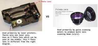
The laser beam must always be in focus to get the highest resolution scans, therefore all laser printers uses a "F-Theta" lens so that the laser beam
focal point will always be in focus for the entire scanning surface. F-Theta lens used in laser printers are specifically designed for 1 axis laser scans only.

Heres the problem, the F-Theta lens found in laser printers are not designed for the UV wavelength lasers such as 405nm. They originally use a different wavelength most likely infrared.

I spent days searching on the internet to find a company/manufacturer that sells these 1 axis F-Theta lens and couldn't find any.
Anyone here knows a company or maybe probably can tell me how I can make my own F-Theta lens used specifically for 405nm lasers?
(Yes, I know many factors must be know such as the polygon mirror size and scanning distance etc... etc)

I do not want to use the multi axis f-theta lens used with galvo scanning motors. I would like to use f-theta lens specifically for 1 axis scans.
Have any other ideas how I can get the focal point always in focus throughout the entire 1 axis?

Please view the attached picture so that you can get an idea what I am talking about.
Also please do not mention about other people's project which is irrelevant to mine, I do not want to use a transparent prism.

Thanks.
 

Attachments

  • Laser_unit_dell_p1500_print.jpg
    Laser_unit_dell_p1500_print.jpg
    807.7 KB · Views: 9


Encap

0
Joined
May 14, 2011
Messages
6,125
Points
113
Sill Optics (Wendelstein, Germany), which produces scan lenses for ultraviolet (UV), visible, and infrared (IR) lasers (both standard and ultrafast), offers both telecentric scan lenses with a perpendicular beam incidence and nontelecentric lenses with high scan fields.

Maybe talk with them perhaps they have or will make what you need/want. See: https://www.silloptics.de/en/products/sill-technicon/laser-optics/f-theta-lenses
 

rajhlinux

Member
Joined
Dec 26, 2020
Messages
67
Points
8
Sill Optics (Wendelstein, Germany), which produces scan lenses for ultraviolet (UV), visible, and infrared (IR) lasers (both standard and ultrafast), offers both telecentric scan lenses with a perpendicular beam incidence and nontelecentric lenses with high scan fields.

Maybe talk with them perhaps they have or will make what you need/want.

I couldn't find the correct naming for f-theta lens that are non-cylindrical.

It seems like everyone in the optic industry likes to call both the "non-cylindrical" and "cylindrical" F-theta lens, without any added differentiation.

Anyways I will get in contact with that company, Thanks.
 
Joined
Sep 12, 2007
Messages
9,399
Points
113
Why is the moderate attenuation unacceptable and not remedied by higher incident power?

We can help you a lot better if you actually tell us about your project rather than a tiny portion of it with seemingly random specifications.
 
Joined
Jan 29, 2014
Messages
12,031
Points
113
Contact these folk, they have had some F-Theta lenses designed for 405 nm in the past, parts from surplus gear they disassembled. If they are out, I know where one is they sold which isn't being used. However, I believe they are closed until Jan 3rd.


rajhlinux

Member
Joined
Dec 26, 2020
Messages
67
Points
8
Why is the moderate attenuation unacceptable and not remedied by higher incident power?

We can help you a lot better if you actually tell us about your project rather than a tiny portion of it with seemingly random specifications.

Honestly I didn't want people to say: "oh, use toner transfer, and call it a day". (This is why I haven't mentioned about the main objective for why I want to build a laser scanning device) I'm sure there are many folks here who fabricates their own PCB at home and doesn't like to wait half a month for delivery.

So yes, basically I'm trying to make a PCB board with the help for LDI "Laser Direct Imaging" technology.
Why do I need such a sophisticated device for etching PCB?

Resolution, Repeatability, Accuracy, Precision, Time and Money.

Yes all of the above 5 reasons will be satisfied with the help of a laser scanning device.
I need mind boggling PCB trace resolution, around 0.05mm. (View the attached image to get an idea).

I do not want to play "hokey, pokey" with toner transfer and burn a finger or two with a cloth iron heater or waste so much ink for printing dozens of transparent film for UV marking. All of the PCB do it yourself at home just seems extremely cretinous and will not work for ultra thin PCB traces for FPGA pins.

Repeatability is only possible with a laser scanning device. I can create a PCB with the help of a laser scanner today with no hassle and repeat the same process the very next hour with no random failures of a copper trace randomly missing or what not.

For those who wants to know the exact details of how I'm going to accomplish 0.07mm PCB copper traces AFTER LASER SCANNING:
(The process is almost similar to how professional PCB fabs makes it)

-Copper clad laminate will be cleaned and polished with a micro etch acid solution with sand paper.
-PCB will be heat Laminated with a "dupont riston" dry film photoresist (Dupont also has special dry film photoresist for extreme resolution given from specifically by a laser scanner).
-Use laser scanner to mark (expose) the UV sensitive photoresist. (The unwanted copper will be cured by the UV laser)
-Use photoresist "developer" to remove the unexposed traces (which is the PCB circuitry).
-Use liquid "Tin" which will be the "Etch Resist" to plate the copper traces so that the "corrosive etchant" does not further attack it, therefore the guarantee of no quality loss of the thin copper traces is accomplished while acid is "etching".
-Use photoresist "stripper" to remove the cured photoresist and expose the unwanted copper.
-Use a special etchant (will be using 30% Hydrogen peroxide + 90% Sulpheric Acid + inhibitors) which will be spray misted and removes the unwanted copper but does not attack the "Tin etch resist".
-Use a special "Tin" "Stripper" solution (which is nitric acid based) to remove the "Tin Etch Resist". (The reason why professional PCB manufactures removes the "tinned" copper traces is so that the growth of "Tin Whiskers" is avoided)
-Use a UV sensitive solder mask (liquid or dry film) to protect the PCB traces (Yes, the UV Laser scanner is needed for this process as well).
-I should have a nice PCB ready to solder SMT components and also solder a nice big fat FPGA with hundreds if not thousands of pins. (Don't get me started how I'll make a 6 multilayer PCB from scratch, yes it's completely doable... that will be for a different forum ;))

So as you can see my deep interest for a laser scanning device.

I have seen few people built such remarkable Laser Direct Imaging devices specifically for PCB.
They obviously know a thing or two about optics, hardware and software (Lets not forget about timing and math...).

Hope someone here can give some advice how I can make such simple but yet advance polygon laser scanner.

So far from my research, I have purchased a "polygon mirror motor" (specifically extracted from a laser printer). I'm waiting for it to arrive.
From my understanding I need few special lens so that the laser will always be in focus to the scanning surface.
I need a collimator and a F-Theta lens this is where I'm lost...
 

Attachments

  • Via-DRC-issues-0.4mm-BGA-Dimensions.png
    Via-DRC-issues-0.4mm-BGA-Dimensions.png
    35.9 KB · Views: 4
Joined
Jan 29, 2014
Messages
12,031
Points
113
They are a rather big, but this is what he was selling, there was one other seller on ebay who had some listed, might still be there.


rajhlinux

Member
Joined
Dec 26, 2020
Messages
67
Points
8
First and foremost Thank you for quick reply.

Yes, I have seen this particular one on eBay few days ago. A used f-theta lens, with some kind of silt at it's input area.

So I am completely puzzled and have no idea how I can use this f-theta lens to work with 1 axis polygon laser scanning mirror.

Have any idea how I can use this f-theta lens? This particular lens is used for multi axis laser beam.

Thanks.
 
Joined
Jan 29, 2014
Messages
12,031
Points
113
I am not sure, bought it to see how multiple beams collimated to infinity would behave through it. In the past, there were also some 405 nm polygonal scanning mirrors this lens came out of for sale from both Starlight Photonics and the ebay seller listing this unit right now, but they were raster scanning mirrors for a display, not a normal mirror. It may appear to have a slit, mine covered in aluminum foil, but it's a normal F-Theta lens, not sure why the mount was machined to look like that, but likely it needed to have one side flattened (which looks like a slit) to properly fit together in the assembly, should work well regardless.
 
Last edited:
Joined
Sep 12, 2007
Messages
9,399
Points
113
Since you've ignored my question entirely, I'll rephrase and elaborate. The lens in an existing laser printer is not opaque to violet light. It will likely have higher attenuation than that of IR light, but why have you determined this attenuation to be unacceptable? Why is your only solution the insistence on buying a 3-figure custom lens?
 

rajhlinux

Member
Joined
Dec 26, 2020
Messages
67
Points
8
Since you've ignored my question entirely, I'll rephrase and elaborate. The lens in an existing laser printer is not opaque to violet light. It will likely have higher attenuation than that of IR light, but why have you determined this attenuation to be unacceptable? Why is your only solution the insistence on buying a 3-figure custom lens?

Well thank you for you interest with my problem for this project.

I have the same question in mind, but I am not an optics expert. I have read and done many research of "LDI" and all the "enthusiast hackers" have said that the lens that are built into the laser printers have no meaningful purpose for 405nm laser. They said that the lens are only good for infrared wavelengths and determined that the attenuation to be unacceptable.

So yes, I'm taking their word for it... But if you want, I can go on craigslist and eBay and buy few used laser printers that are just being thrown away and I can extract the lens and polygon motor module and actually verify the len's attenuation for 405nm on my own.

Because of this I insisted to contact numerous companies for this special f-theta lens which is oddly shaped like a bar. Hoping that they can supply one in the range of 405nm.

I guess I'll start hunting for some thrown away laser printers on craigslist... I'm assuming your knowledge with optics is great because of your
skepticism of the built in lens should work with 405nm laser.

Here is some references where "enthusiast hackers" said that the built-in lens are not worthy (yes, resolution, repeatability, precision and accuracy are the best interest in mind from all of these people):

wiki.das-labor.org/w/LaserExposer
youtube.com/watch?v=G9-JK2Nc7w0
hackaday.io/project/21933-open-hardware-fast-high-resolution-laser
youtube.com/watch?v=fi4P-Bwc6g8&list=PLFVpu85GvZwRz4vTu39MPfUwYSSYG5SP-
youtube.com/watch?v=KpM0LJLToJU&t=25s
 
Last edited:

gazer101

Well-known member
Joined
Feb 23, 2020
Messages
700
Points
63
Test it out, its always logical to buy something cheap that might work before assuming it won't work and going for the more expensive option :)
 

rajhlinux

Member
Joined
Dec 26, 2020
Messages
67
Points
8
LAser scanning unit.jpg

Alright so I just purchased a used "Laser Scanning Unit" for a "HP LaserJet M2727nf", it was the lowest price I could find on eBay that is advertised as good working condition and not stated as refurbished. This particular LSU can scan at 1200 DPI horizontally, which is pretty much high resolution.

I also have a fully functional "Brother HL-2270DW" laser printer that is collecting dusts for the past 6 years... I'm really tempted to disassemble it and extract the laser scanning unit... Obviously once I open it, I'm never going to assemble it back into good working order, since I bought this laser printer used from craigslist about 6 years ago, therefore not worth my time to assemble it back.
I already have two printers that are being used at the moment one is an inkjet and another is also a different brother laser printer.

I guess I'll just wait for the HP printer LSU to arrive (about two weeks...:cry:)...
Meanwhile I can study about building the laser's driver module for switching it.
 
Joined
Sep 12, 2007
Messages
9,399
Points
113
From my (exceedingly limited) knowledge on lithography, the exposure is energy-dependent, not power dependent. Yes? Even with a 50% attenuation, doubling power or doubling exposure time negates this, yes?


Top