Hi guys,
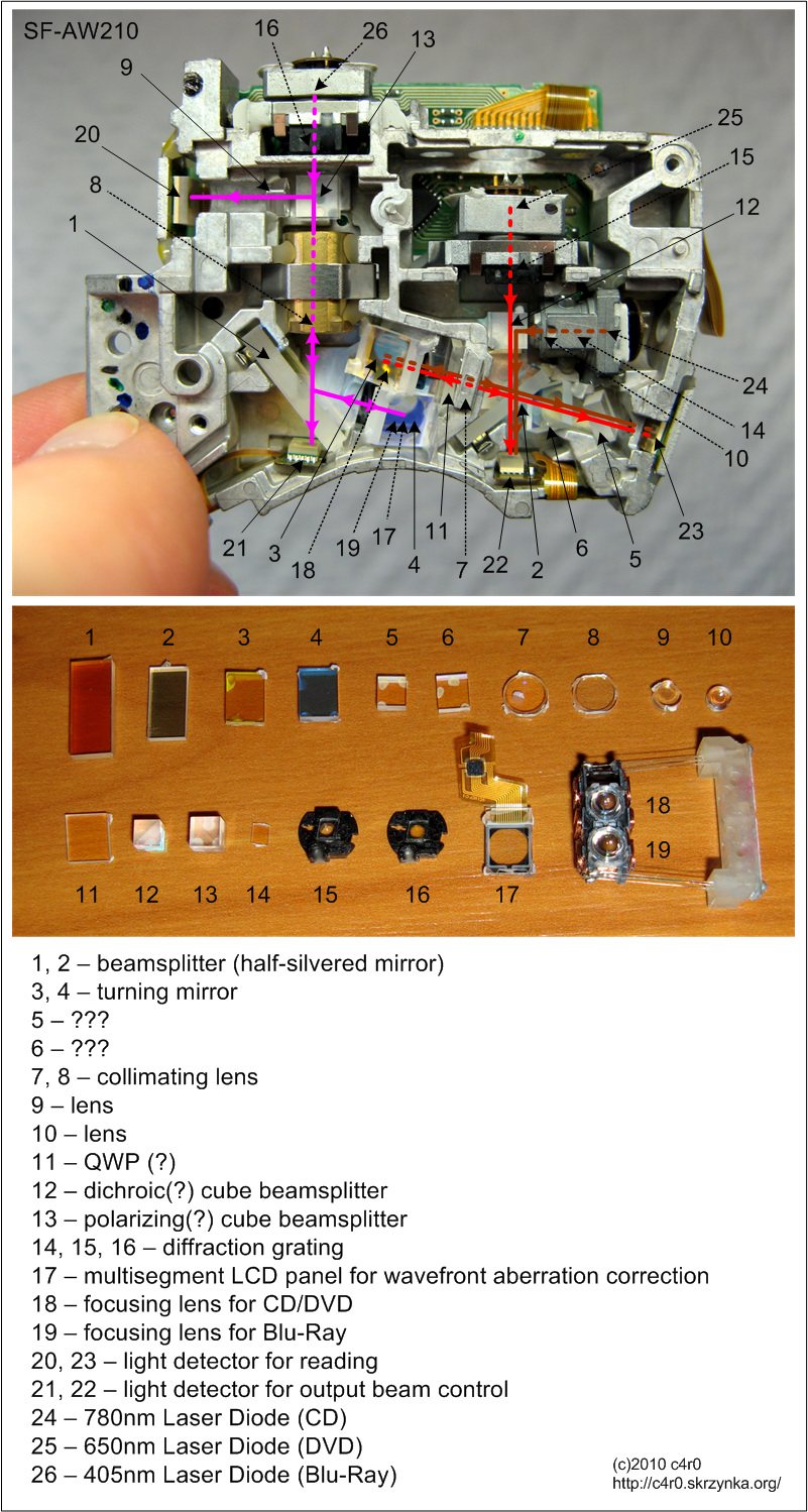
I know you all know where to find good information on the topic. For an experiment, I decided to use a diode sled (SF-AW210) in order to expose photoresist, and it worked very nicely. The question that I had is why is there a diffraction grating right after the BD 405 nm diode, for example, the grating marked as #16 in this image:

Can anyone post some link as to where I can find information on it? For my experiment I removed it since I saw no purpose to it, but I want to be sure.
Thanks in advance!
Alan
I know you all know where to find good information on the topic. For an experiment, I decided to use a diode sled (SF-AW210) in order to expose photoresist, and it worked very nicely. The question that I had is why is there a diffraction grating right after the BD 405 nm diode, for example, the grating marked as #16 in this image:

Can anyone post some link as to where I can find information on it? For my experiment I removed it since I saw no purpose to it, but I want to be sure.
Thanks in advance!
Alan
Last edited:


