Welcome to Laser Pointer Forums - discuss green laser pointers, blue laser pointers, and all types of lasers

LPF Donation via Stripe | LPF Donation - Other Methods

Links below open in new window

ArcticMyst Security by Avery

520nm 750mW Green laser "gun?".

Marecek

New member
Joined
Feb 2, 2020
Messages
7
Points
3
Hey, everybody,
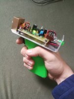
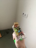
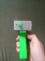
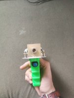
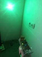
This is probably my first post so I'd like to show my better side. I would like to show my latest project regarding lasers. It's a 520nm 750mW laser.
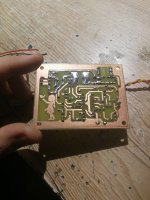
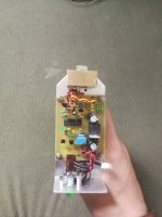
It is completely my design including 3D prints, switched CC converter and complete test and diagnostics. Before I get to the description of the CC converter though, it is an aluminum structure that serves as the heat sink and frame of the entire device. The 520nm TO9 laser diode is housed in a G2 lens optic and the whole thing is encased in a brass die. Hidden inside the green handle is a push button and a 3S LiPo 450mA/h battery (for models).
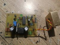
So, to get to the inverter, it is a switching step-down inverter with a current loop. It's designed to minimize ripple and protected so that in the event of a fault, the full battery current won't enter the diode. The control of the step-down converter I have 0 - 100% duty cycle. To protect the laser diode I have an integrated softstart with pushbutton input. The softstart is about 250ms long.
The switching power supply works from 7 - 20v and the output currents specifically for this piece I made 150 - 1900mA, but after changing the shunt you can go up to 20A.
So hope you like it and have a great rest of the day everyone. Regards Marecek 😸 .308956842_433375518861944_244799471849503607_n.jpg309060791_434273088800733_8599892627248858138_n.jpg

309136557_1256858808431836_915547201391381843_n.jpg309113779_538738867722731_6556563464504775950_n.jpg308807957_462031572616535_6024026524705771443_n.jpg308755781_777702633345972_6163154941145914866_n.jpg308726450_659793235369022_7773964126988546589_n.jpg309202693_679750680327581_8203603663636537317_n.jpg


farbe2

Well-known member
Joined
Oct 3, 2018
Messages
303
Points
63
Nice work!
Especially the circuit board. Not many people that etch there boards themself anymore.

However I would not recommend running the board at 20A. even 10A would be a little much.
The Mosfet switch might be able to handle that. However your inductor would be in saturation and your traces will get way to hot.
I see that you added solder to the traces to beef them up. Sadly this does not increase the current carrying capability by much.

EEV Blog got a nice video on YT about this topic. (including measurements)

Dont be afraid of SMD components, I find its much less work to do a PCB with them as i dont need to drill holes.
I also find soldering of SMD not soo hard. Stick with 0603 or above and its easy to solder.

I like the easteregg drawing you got there :D.

Do you mind sharing your etching process? (toner transfer / mask expose?)
Also: what software did you use to make the PCB?
 

Marecek

New member
Joined
Feb 2, 2020
Messages
7
Points
3
Nice work!
Especially the circuit board. Not many people that etch there boards themself anymore.

However I would not recommend running the board at 20A. even 10A would be a little much.
The Mosfet switch might be able to handle that. However your inductor would be in saturation and your traces will get way to hot.
I see that you added solder to the traces to beef them up. Sadly this does not increase the current carrying capability by much.

EEV Blog got a nice video on YT about this topic. (including measurements)

Dont be afraid of SMD components, I find its much less work to do a PCB with them as i dont need to drill holes.
I also find soldering of SMD not soo hard. Stick with 0603 or above and its easy to solder.

I like the easteregg drawing you got there :D.

Do you mind sharing your etching process? (toner transfer / mask expose?)
Also: what software did you use to make the PCB?

Thank you for liking one of my lasers.

I've been doing panel joints since I was a kid, although I draw boards at work and have them done in JLCPCB. However, at home I make them using etching.

Sure, the board would want to accommodate stronger components like mainly diode, inductor, low ESR capacitors and more blocking. Of course, this also applies to current sensing where I would probably already solve it with a LEM or smaller shunt value with a differential amplifier. I would probably design a switching power supply with synchronous rectification and much higher frequency for higher efficiency, and adapt the inductor to higher skin effect sensitivity and core gap.

Sure, if there would be a specific link to the YT one ? I deal with switching power supplies, power supplies and the like, of course my focus on electronics is much broader, but here in this article I'll stick to switching and linear power supplies.
However, in the future I will be designing a general purpose switching buck/boost converter from discrete components. Of course I could use a ready-made integrated circuit that is designed for this, but I like to learn, I like to design my own and it is more affordable from conventional components.

To answer your message completely, I want to do it in SMD too, I have no problem with design, soldering and assembly, I also work with 0201 size and BGA bushings. In home conditions I would definitely go in 0603, just that at home I have mainly THT components and SMD only minimum. However, what bothers me in home SMD is that it needs proper PCB design and interconnects between layers. In this THT case, I didn't use a single jumper and the design meets everything a switching converter should have and that is very important for these purposes.
But I will definitely do an improved version in SMD and it will appear here in the future.

Yeah, my logo :D it's for a longer explanation, however I have another one in the form of a heart. But I'm glad you like it.

In this case, I went the photo route, i.e. transferred the PCB sketch to paper, sprayed with WD spray for transparency, illuminated with UV on the photosensitive CU PCB, rinsed it in developer (Sodium Hydroxide 10%, water 90%) and then etched in ferric chloride. Not to forget drilling the holes, soldering the parts and spraying on the protective varnish.
I have more ways of doing this though, like burning toner, milling or drawing with an alcohol marker.
I use several types, Eagle, KiCad, Sprint Layout, EasyEda, Altium or plain square paper and a regular pencil.

I hope this isn't a long description :D if you have more questions, feel free to ask. Regards Marecek.
 

farbe2

Well-known member
Joined
Oct 3, 2018
Messages
303
Points
63
I also work as a electronic designer mainly focused on efficient dc/dc supply stuff.

I dont etch anymore. JLC is too fast and affordable to not use it.
I currently work on a very very small dpss laser driver (diode and 2x tec) with synchronous stepdowns for everything.
I used ICs as I am going for small not cheap.
Everything 0402.

I used to etched pcbs with natriumpersulfate as its not as "dirty" and you can much easier see what's going on in the bath.
Photo transfere was my preferred route. Most of the time I used the sun to expose the circuits.
WD40 for transparency is neat. I used sunflower oil but that made bubbles while exposing resulting in a lifted off mask and therefore unsharp images.
I am not sure if the bubbles are gasses produced by the exposure process / reaction of the substrate with the uv light or if the sunflower oil reacts with something.

I will try the WD40 trick if I ever need to make boards again.


Top