Welcome to Laser Pointer Forums - discuss green laser pointers, blue laser pointers, and all types of lasers

LPF Donation via Stripe | LPF Donation - Other Methods

Links below open in new window

ArcticMyst Security by Avery

Dave is Mean to his Diodes (445 Macros) IMAGE HEAVY

Joined
Aug 25, 2007
Messages
2,007
Points
63
So yeah, I got this diode from theMonk, who got it from daguin. It's supposedly a "zombie", but I haven't powered it on to look, but I'll trust them.

If it is lasing, I'm freakin' impressed. I've watched this kind of damage happen to a diode under a microscope before, watching as it happened. It's not pretty, but it is pretty awesome to watch. So yeah, here are some macros of this diode that Dave treated so cruelly. Enjoy!

WARNING: These images of diode carnage are not for the faint of heart. If you care deeply about diodes and can't stand destruction, look away. You have been warned.

Oh, and sorry they're all upside down, the light worked better that way. And the color balance is screwy on many of them, so yeah, sorry.

--------------------------------------------

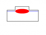
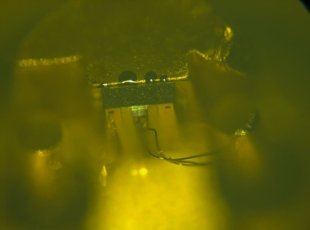
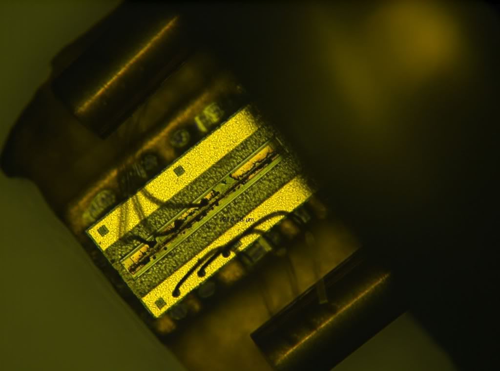
First, the typical 45deg shot. You can see the pedestal, the base the diode is mounted on, some bonding wires, and the front facet of the diode. Depth-of-field sucks, so that's all you can see. Can't see any damage yet...

5x_45deg_hires.jpg


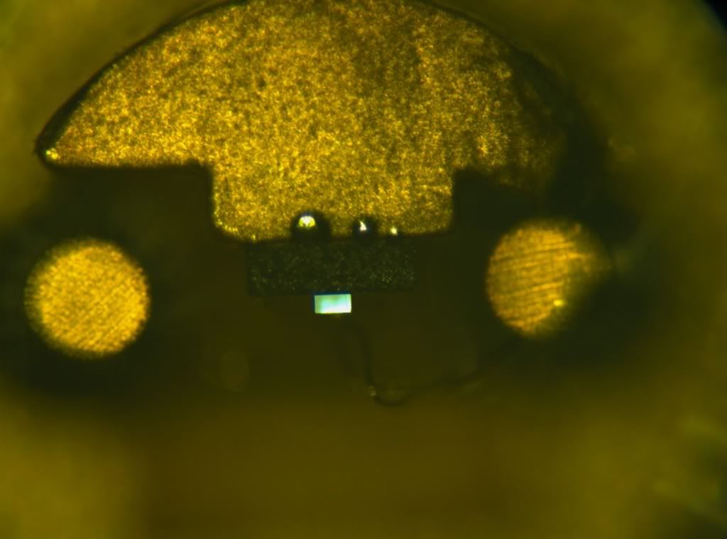
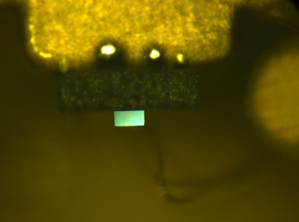
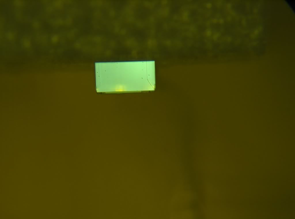
Next, an end-on view of the facet of the diode. A pretty sweet image. The facet is the bright part.

5x_facet_hires.jpg


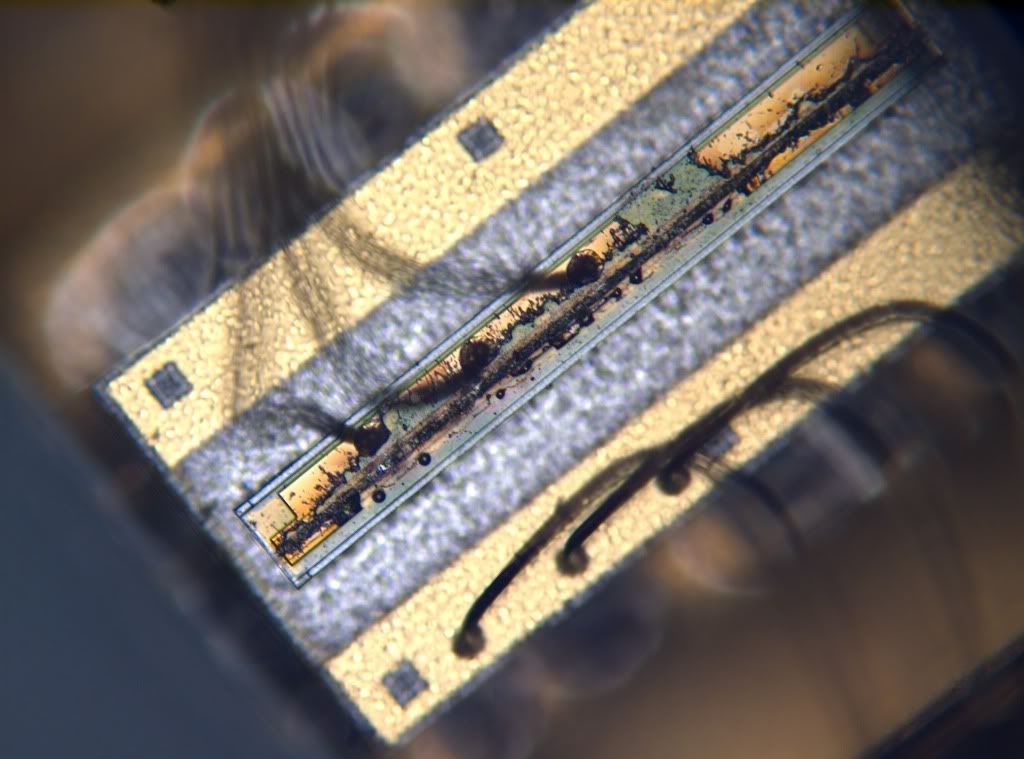
And now, a low-mag top-down image of the diode, totally cringe-worthy

5x_topdown_3_hires.jpg


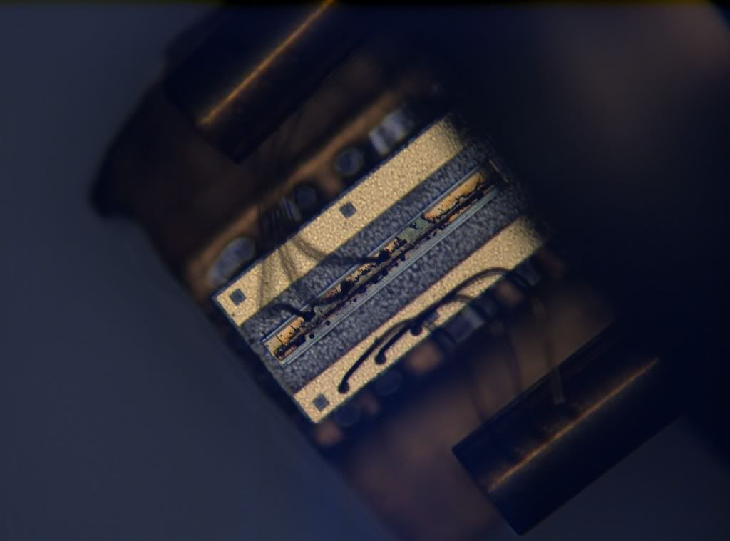
And the same image, apologies for the color balance, but with a handy scale bar. In case you can't read it, the die is about 1200 microns long.

5x_topdown_2_hires.jpg


Moving on, next magnification, again a view of the diode's front facet. Not a bad image at all.

10x_facet_hires.jpg


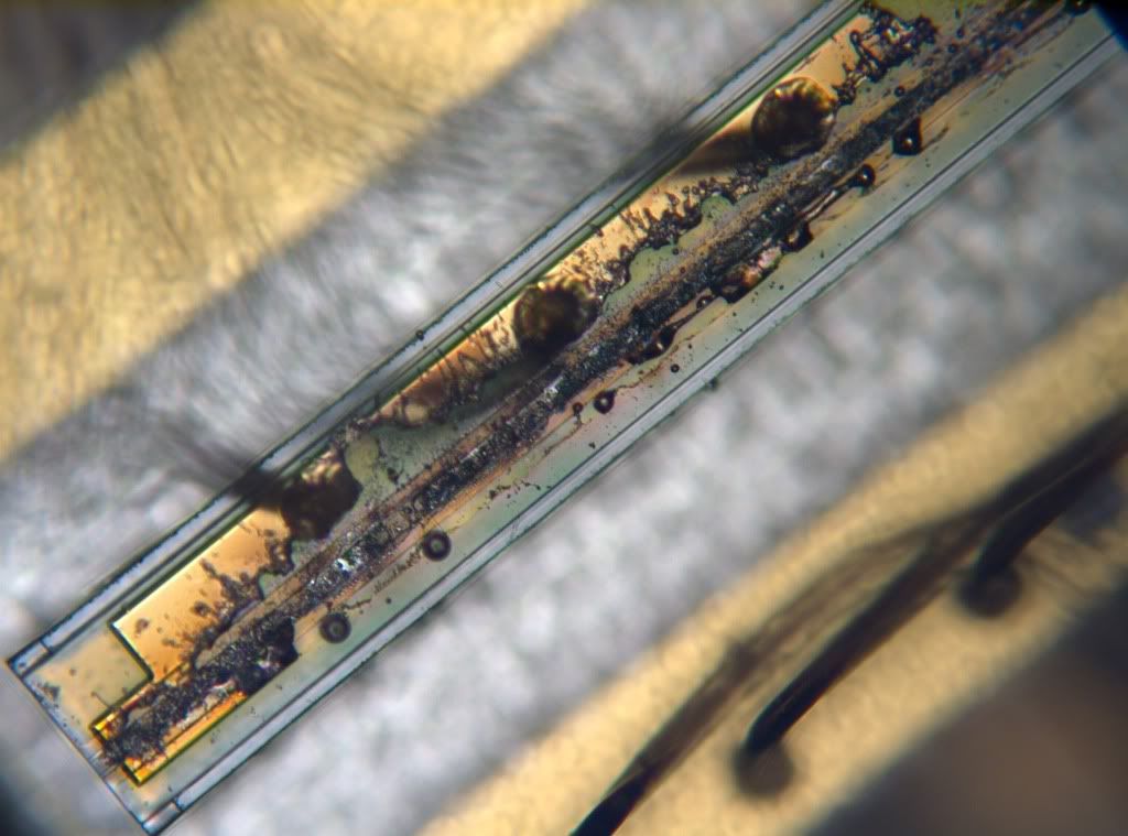
And, the next image is the same magnification, again top-down. Ouch. Yeah, this diode went through a terrible event in its life. I anticipate intensive therapy for the rest of its life.

10x_topdown_2_hires.jpg


One more top-down image, zoomed in a bit on the top facet. Even through all the destruction, you can see some of the interesting bits of the diode's structure (especially down in the bottom left hand corner of the image where the output facet is) related to an on-going thread in the Science sub-section regarding multiple lateral mode diode.

Sadly, this is just the 3rd of 6 magnification levels available. I was able to use all 6 objectives on the facet (see below), but not on the top-down view. In order to use the 3 higher magnifications, I'll have to remove the diode from the 5.6mm can base, because that base prevented the objective from getting close enough to see the diode, since the working distance gets to be much less than 2mm.

20x_topdown_4_hires.jpg


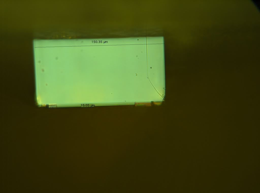
And now, zooming in on the facet of the diode. This is the 3rd magnification level. Curiouser and curiouser.

20x_facet_hires.jpg


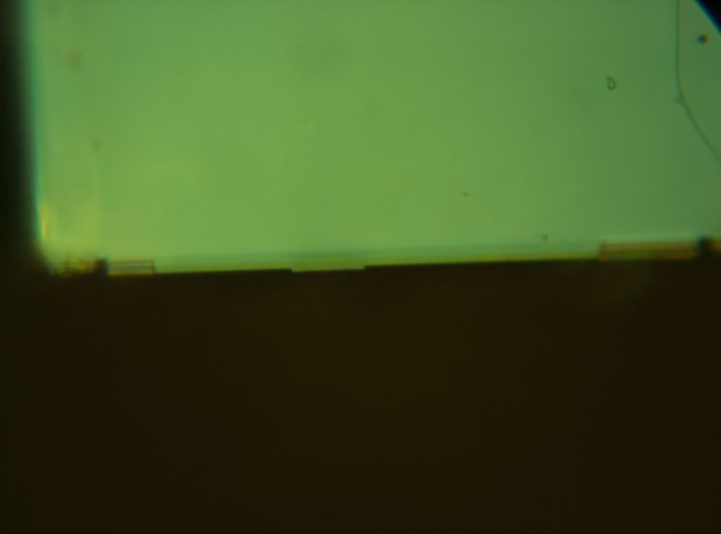
4th magnification level. I see a ridge there....

50x_facet_hires.jpg


Same, with some scale bars.

50x_facet_2_hires.jpg


5th magnification level.

100x_facet_hires.jpg


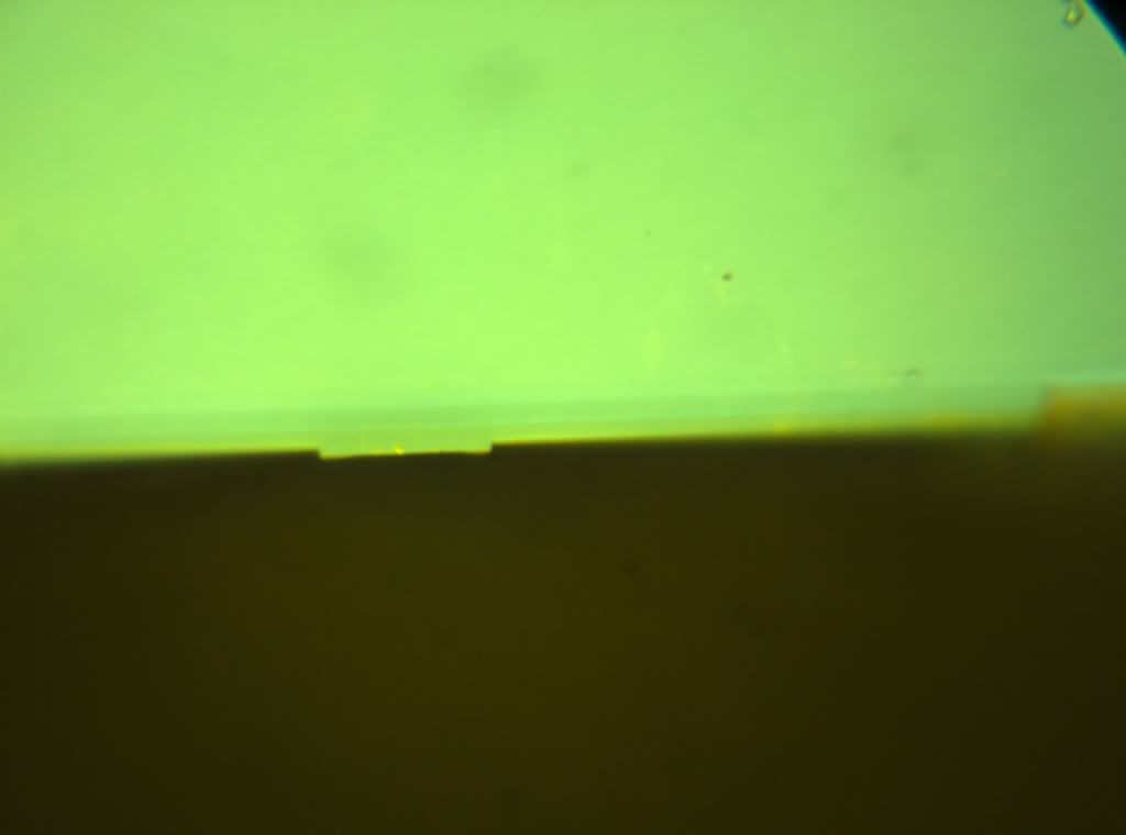
And 6th and final level of magnification. Yep, that's a 15 micron ridge there for some later waveguiding of some kind. And some pretty impressive imaging, if I do say so myself. A little bit of tinkering/deconstructing, and this level of magnification may be achievable in the top-down view. Then of course, there are also electron microscopes as well.

150x_facet_hires.jpg


Joined
Nov 17, 2009
Messages
2,031
Points
83
Wow. It seems like where the bonding wires make contact, that 'plate' has almost been eaten away, but if it's still lasing - likely enough remains to make enough contact with the p/n junction...

I guess it's when the facets go, thats when it goes LED. But it seems that everything AROUND the die has gotten incredibly hot, but the die has survived...

He did say this one still lases?, is that right?
 
Joined
Sep 20, 2008
Messages
17,622
Points
113
From the metal splatter on the top of the Die...
I would really be surprised if it had any type of output..

@PBD.... nice macro photos... the top of the die shots
are amazing...

Jerry
 
Joined
Sep 16, 2007
Messages
3,658
Points
113
Pictures are awesome.

I have a "zombie" de-canned 405 (LG 8X burner). It will still lase. Last I measured, It's still producing ~300mW at random current (between 200 and 300mA, I think 260). The beam profile sucks, though. Looks like this: (0).

I don't really have any use for it besides reminding me that I cooked $200. Does you or anyone else have any use for it?
 
Joined
Aug 25, 2007
Messages
2,007
Points
63
He did say it still lases.

Basically what has happened is the metal contact pad, which is most likely deposited by some process like electron-beam evaporation or sputtering, has been blown off of the diode in most places. I've seen it happen live in a microscope. When it happens, it looks almost like bolts of lighting shooting through the diode, from one end to the other, you can watch it race through delaminating/throwing the metal off. It leaves pits, craters, metal pieces. There's still metal there making contact in places, and the metal is pretty far from the light (relative to the size of the light, that is) in the diode anyway, so the active region is maybe not physically damaged, but who knows? But getting the current into the diode is tough when you've blown all the contact metal off the device.

Making metal to p-type doped GaN is notoriously difficult. It's hard to get an Ohmic contact, so you very often end up with a mini Schottky diode where the metal touches the semiconductor. This can absorb heat, bad things can happen, etc. It's a weak point, and it breaks sometimes.
 
Last edited:
Joined
Dec 23, 2007
Messages
2,494
Points
0
That's pretty cool! I needed some of these measurements for my 3d model of this diode!
 
Joined
Jan 12, 2008
Messages
3,290
Points
83
Best pictures ever taken. Ever.

Is the laser output coming from that 15 micron ridge?
 
Joined
Dec 21, 2008
Messages
1,223
Points
0
Great work, PBD! Do you have a camera system directly connected to a professional microscope?
 
Joined
Aug 25, 2007
Messages
2,007
Points
63
Great work, PBD! Do you have a camera system directly connected to a professional microscope?

Thanks. I had a legitimate work interest in this, so I didn't mind using work tools. I don't use work tools for personal gain, but since I had a work interest in these, I figured you guys could benefit a little as well.

And so yes, these images were taken using something akin to this

eclipse_l200sm1.jpg


plus this.

imageTET.JPG


Best pictures ever taken. Ever.

Is the laser output coming from that 15 micron ridge?

Thanks!

And kinda, yeah. Laser diode makers etch the ridge to form a lateral waveguide, but you don't etch all the way through the active region, so the active region is actually still in the bulk below the ridge, not "within" the ridge. The mode(s) would be located somewhere kinda like this attachment. This is not to scale and is approximate in every way, but shows the idea of hoe most of the mode is not within the ridge, but the ridge still acts to confine the mode. The mode is in red, with active region is the blue line. Without the ridge, the mode would spread out to the right and left much wider. The height of the mode is controlled by putting different layers in, and not as much by the ridge itself.

So yeah, the light is all coming out just "below" (above in my upside-down images) the ridge. Puts it into perspective, eh? The actually emitting region is still just a tiny fraction of the die; even in the last image with such huge magnification, the actual part where there is laser emission is still small.

This ridge is 15um wide, which is why it is multiple lateral modes. For single mode diodes, like everything that comes out of an optical storage drive (405nm, 660nm from Blu-Ray and DVD), that ridge is narrower, like 1 or 2 um wide. The PHR diode has a 1.5 micron ridge, for instance.

Oh, and duh, the ridge has another purpose: current guiding! The best way to do it is to inject current only straight down through the top of the ridge. So if all the current is coming in through the ridge, as much of it as possible goes into the optical mode. For stimulated emission, you need the light and the current both in the same place, so this helps to ensure that all the current ends up in the same place as the light. Which points out another cool thing about these devices: ALL the current you're putting in is passing through that ridge, which is 15 microns wide and 1200 microns long. The current comes in through the wires, flows laterally through the metal film, and then straight down through that small ridge.
 

Attachments

  • RidgeLaser.PNG
    RidgeLaser.PNG
    4.9 KB · Views: 1,490
Last edited:

daguin

0
Joined
Mar 29, 2008
Messages
15,989
Points
113
VERY cool! :thanks:

The diode was still producing ~200mW at high current when I sent it to The Monk

Peace,
dave
 
Joined
Aug 25, 2007
Messages
2,007
Points
63
Thanks, Dave.

Also, I just did another little calculation based on some other info I had forgotten....

With diodes and how they break, it's often not so much about current as it is about current density: as in how much current is flowing through the area of the diode.

So this diode is 1200um x 15um. Somebody check my math here, but I get that working out to ~.00018 cm^2. Pushing 1A of current through this gives a current density of ~5.6 kA/cm^2. Believe it or not, that's a low number.

Let's compare to the PHR: the PHR is ~ 400um v 1.5um, giving an area of .000006 cm^2. At a typical operating current of .1A = 100mA, that gives a current density of, get this, ~16.7kA/cm^2.

So at least as far as current density, these things actually operate at a pretty low number, despite the fact that they operate at such huge currents. The threshold current density is, well, it's impressive. I know 200mA seems like a lot of current, but it's really not much at all when you look at how big the diode is. The PHR's threshold current density is higher than the operating current density of this diode when driving it with 1A of current.

There are a LOT of differences though with different diodes, so please don't read much into this post, other than to say I'm impressed with these diodes. Unless my math is wrong? Can anyone else check it?
 
Last edited:
Joined
Dec 23, 2007
Messages
2,494
Points
0
Is it just possible they can be pushed further than 1A?

I don't know enough about diode workings to have a serious intellectual conversation :D
 

daguin

0
Joined
Mar 29, 2008
Messages
15,989
Points
113
Is it just possible they can be pushed further than 1A?

I don't know enough about diode workings to have a serious intellectual conversation :D


We are pushing them past 1A regularly now

Peace,
dave
 
Joined
Sep 16, 2007
Messages
3,658
Points
113
@Pullbangdead,
When constructing diodes for high power, what exactly is it that makes them more robust?

How is it that we can "kill" these diodes and still get it to lase at close to "normal" outputs? And how does it affect the emitted modes?

Up until I "killed" my 8x, I had never witnessed a "zombie" failure. Most of us have witnessed the "LED effect," and I've burned up a diode to no output, but I'm having trouble understand what has to be damaged for a diode to go "zombie."
I mean... if I look at my zombie 8X under a microscope should it look similar?
 
Joined
May 4, 2009
Messages
2,238
Points
83
Really awesome pictures. I sure wish i had a microscope, the microscopic world looks pretty neat


Top