Welcome to Laser Pointer Forums - discuss green laser pointers, blue laser pointers, and all types of lasers

LPF Donation via Stripe | LPF Donation - Other Methods

Links below open in new window

ArcticMyst Security by Avery

A-140 vs. M-140 vs. H1600

Joined
Aug 25, 2007
Messages
2,007
Points
63
Oh yeah, and because I know some of you care, (and for teh lulz).....these diodes aren't made by Nichia.
 
Last edited:


Joined
May 25, 2010
Messages
3,655
Points
0
Oh yeah, and because I know some of you care, (and for teh lulz).....these diodes aren't made by Nichia.

Are you talking about the 9mm or the 5.6mm ones or both.?

I had a Pretty good Idea the 5.6mm ones where Not but the 9mm ones i thought they where.


Per your Question of the Black Line Across the Facet:

The Black Line across the Facet is COD.
 
Last edited:

jayrob

0
Joined
Sep 21, 2007
Messages
9,862
Points
113
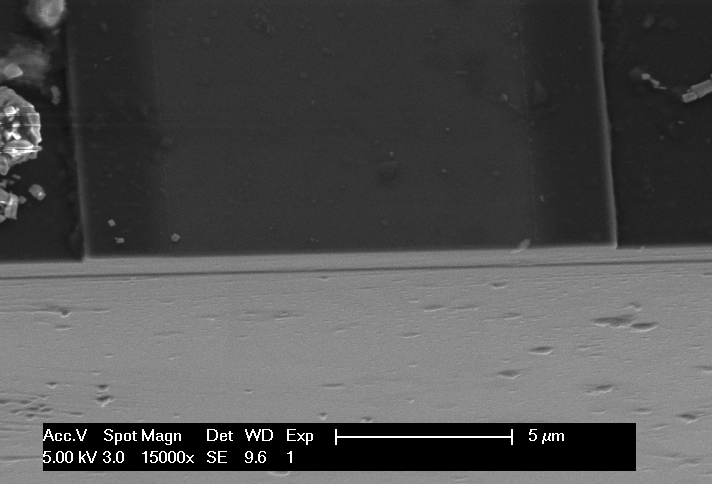
And this image is cool. It shows something interesting, and taught me something as well. Somebody guess what the horizontal black line is on the facet of the diode.

3.png


The line is so perfectly straight. Maybe it is an alignment mark??
 
Joined
Jan 2, 2009
Messages
11,800
Points
0
Its a specularly reflecting plane.

A scratch made at the edge of the wafer and a slight bending force causes a nearly atomically perfect mirror-like cleavage plane to form and propagate in a straight line across the wafer.
 
Joined
Aug 25, 2007
Messages
2,007
Points
63
Are you talking about the 9mm or the 5.6mm ones or both.?

I had a Pretty good Idea the 5.6mm ones where Not but the 9mm ones i thought they where.

None of them are from Nichia.

Per your Question of the Black Line Across the Facet:

The Black Line across the Facet is COD.

Nope.

The line is so perfectly straight. Maybe it is an alignment mark??

Nah. It is spectacularly straight though, you're right.

Its a specularly reflecting plane.

A scratch made at the edge of the wafer and a slight bending force causes a nearly atomically perfect mirror-like cleavage plane to form and propagate in a straight line across the wafer.

Nah. It's not visible in the optical images, only in the electron microscope image.

What you're talking about is done, you can see it on the top corners of the 2nd and 3rd optical microscope images. Those images are looking at the facet, and you can see on the corners where they scribed from above in order to cleave the facet. They don't scribe on the ridge itself, they scribe between lasers and then cleave between the scribes to form the facets.
 
Joined
May 10, 2011
Messages
1,878
Points
48
will someone explain to me how i missed this thread ? :wtf:

thank you kind sir pullbangdead for the fantastic pictures and information these are the threads i LOVE
 
Joined
Aug 25, 2007
Messages
2,007
Points
63
BTW, my inner 6-year-old was loving that. "I know something you don't know!!1!". Because let's face it, who isn't beholden to their inner 6-year-old at times?

But seriously, it's cool: It's the active region, the quantum wells. How cool is that?

Take all the images together, for scale. On the last optical 'scope image, you can barely see that 15um ridge, and the active region tis tiny even when compared to the ridge. And all the laser light leaving the device, every photon, is coming out of that tiny little line, and only under the ridge you see there.

Of course you have to remember to think in 3D, the active region extends out over the entire device. But still, it's thin.
 
Joined
Dec 27, 2011
Messages
2,062
Points
48
And I'm very disappointed this got no response. Nothing? A black line on a high-mag sem image of the facet of a laser diode?

I had no idea and decided to go with "keep my mouth shut and look stupid" rather than "open my mouth and remove all doubt.". :D

BTW, I can't find that microscope on Amazon or EBay... Do you have a link? :crackup:


BTW, my inner 6-year-old was loving that. "I know something you don't know!!1!". Because let's face it, who isn't beholden to their inner 6-year-old at times."

I think it is safe to say that anyone on this site who is making, buying or playing with laser pointers is "beholden to their inner 6-year-old" a lot of the time!
 
Last edited:

Hiemal

0
Joined
Dec 27, 2011
Messages
1,443
Points
63
It truly amazes me how they can pump these diodes out for such a low price.

Why's that? I don't see any reason why they wouldn't be able to.

I mean, they have automated machines that make these. The process of making silicon is relatively easy, and well sand isn't exactly a non-renewable resource considering how much sand we have.

And because it's automated I'd imagine it'd be cheap to make thousands of these...
 
Joined
Jan 2, 2009
Messages
11,800
Points
0
I know the actual material is cheap. I was thinking the cost of R&D, and engineering the equipment to work at such a minute level.

Sometimes I forget how big the diode market is, and where they are created. You could never get a price close to what we pay for if they were made in the US.
 
Joined
Jan 2, 2009
Messages
11,800
Points
0
Well, cheap for what we use them for.

You can buy a green laser for $5. Which shows they only pay ~$1.
 
Joined
Dec 27, 2011
Messages
2,062
Points
48
Well, cheap for what we use them for.

You can buy a green laser for $5. Which shows they only pay ~$1.

Yeah, I was just kidding anyway. They are cheap. Figure there are a couple dozen in a projector that costs a grand or so and that is only a PART of the projector, they can't cost more than a few bucks to the projector maker.
 
Joined
Aug 25, 2007
Messages
2,007
Points
63
Why's that? I don't see any reason why they wouldn't be able to.

I mean, they have automated machines that make these. The process of making silicon is relatively easy, and well sand isn't exactly a non-renewable resource considering how much sand we have.

And because it's automated I'd imagine it'd be cheap to make thousands of these...

The cost of silicon has nothing to do with it, because these diodes aren't made of silicon. The only silicon in the whole diode is the n-type dopant, which is a miniscule amount in only part of the diode.

They're made of gallium nitride, which is very difficult to make, and a heck of a lot more expensive than silicon.
 

Hiemal

0
Joined
Dec 27, 2011
Messages
1,443
Points
63
*facepalm*

That's right, sorry. I'm thinking of standard diodes... xD

Then, in that case, I do rather wonder how they can manufacture them so cheaply.

Perhaps it is still due to the "automated" aspect of it?


Top