Two excerpts from Sam's Laser FAQ about vertical surface emitting laser (vcsel). Reading over the simplified manufacturing I wonder why we're not seeing inexpensive vcsels offered by our favorite companies?
http://www.repairfaq.org/sam/laserdio.htm#diocss8
Most laser diodes up till now (as well as most of those discussed in this document) are edge emitters - the beam exists from the cleaved edge of the processed laser diode chip. These are also called Fabry-Perot (FP) diode lasers since the cavity is essentially similar to that of a conventional gas or solid state laser but formed inside the semiconductor laser diode chip itself. The mirrors are either formed by the cleaved edges of the chip or (for high performance types like those that are very stable or tunable) one or both of these are anti-reflection (AR) coated and external mirrors are added.
VCSELs, on the other hand, emit their beam from their top surface (and potentially bottom surface as well). The cavity is formed of a hundred or more layers consisting of mirrors and active laser semiconductor all formed epitaxially on a bulk (inactive) substrate.<br>
This approach provides several very significant technical advantages:
Beam characteristics - Much of the behavior of the VCSEL can be controlled or at least affected by selecting the number and thickness of mirror layers and other process parameters. The potential capabilities of this technology to finely tune behavior is hard to imagine. VCSELs operate in a single longitundinal mode but possibly multiple transverse modes.
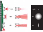
Beam shape and profile - Whereas the typical conventional low power FP laser diode has an emitting area of 1x3 um (they are all long and narrow because the junction where laser action takes place is almost zero thickness), the shape of the emitting region of a VCSEL can be made whatever is desired for the application - even in the form of a doughnut or ring for optimal coupling to the outer part of a multi-mode optical fiber.
The beam from a typical VCSEL exits from a circular region 5 to 25 um in diameter. Since this is much larger than for the FP laser diode, the divergence of the resulting beam is much lower. And, because it is also circular, no corrections for asymmetry and astigmatism are required - a simple lens should be able to provide excellent collimation.
Lower lasing threshold and drive current - A typical telecom or CD laser diode may have a threshold current of around 30 mA while a VCSEL with similar output power may require only 1 or 2 mA! This results in lower electrical power requirements, potentially faster modulation, simpler drive circuitry, and reduced RFI emissions. VCSELs are also more robust in terms of power supply drive. Current control is generally sufficient and there is no need for optical feedback using a monitor photodiode to prevent destruction as with most low power edge emitting laser diodes where COD (Catastrophic Optical Damage) can occur in a ns as a result of the peak optical power at the 1x3 um output facet. With VSCELs, the emitting area is much larger so COD isn't nearly as significant a problem.<br>
Implementation of VCSEL arrays becomes trivial. All that is required is to dice up the wafer into blocks of adjacent good VCSELs and package these as a single unit. The packing density of such devices can be an order of magnitude higher than for FP laser diodes (see below). This is a significant advantage for constructing high speed optical busses and interconnects.
There are also numerous manufacturing and cost advantages:
Smaller size - Unlike the FP cavity of an edge emitting laser diode which is 250 to 500 um in length, the entire size of a VCSEL is limited by the dimensions of the emitting region and space for electrical contacts. Thus, the die for a complete VCSEL can potentially be only slightly larger than the beam size! Currently available devices with a 25 um circular beam are about 100 um on a side but this can certainly be reduced to 50 um or less. Smaller size can translate into a larger yield per wafer and lower costs as well a higher packing densities for laser array applications.
Simplified manufacturing and packaging. Virtually the same equipment that is used for final assembly of devices like other ICs can be used for VCSELs since they are attached flat on the package substrate and shine through an window like that of an EPROM (but of higher optical quality) or merged with an optical fiber assembly as required. Since the active lasing semiconductor and mirrors are buried under the top surface layers, a hermetic seal is unnecessary. VCSELS can use inexpensive plastic packaging and/or be easily combined with other optical components as a hybrid or chip-on-board assembly. All this further contributes to reduced cost.
http://www.repairfaq.org/sam/laserdio.htm#diocss8
Most laser diodes up till now (as well as most of those discussed in this document) are edge emitters - the beam exists from the cleaved edge of the processed laser diode chip. These are also called Fabry-Perot (FP) diode lasers since the cavity is essentially similar to that of a conventional gas or solid state laser but formed inside the semiconductor laser diode chip itself. The mirrors are either formed by the cleaved edges of the chip or (for high performance types like those that are very stable or tunable) one or both of these are anti-reflection (AR) coated and external mirrors are added.
VCSELs, on the other hand, emit their beam from their top surface (and potentially bottom surface as well). The cavity is formed of a hundred or more layers consisting of mirrors and active laser semiconductor all formed epitaxially on a bulk (inactive) substrate.<br>
This approach provides several very significant technical advantages:
Beam characteristics - Much of the behavior of the VCSEL can be controlled or at least affected by selecting the number and thickness of mirror layers and other process parameters. The potential capabilities of this technology to finely tune behavior is hard to imagine. VCSELs operate in a single longitundinal mode but possibly multiple transverse modes.
Beam shape and profile - Whereas the typical conventional low power FP laser diode has an emitting area of 1x3 um (they are all long and narrow because the junction where laser action takes place is almost zero thickness), the shape of the emitting region of a VCSEL can be made whatever is desired for the application - even in the form of a doughnut or ring for optimal coupling to the outer part of a multi-mode optical fiber.
The beam from a typical VCSEL exits from a circular region 5 to 25 um in diameter. Since this is much larger than for the FP laser diode, the divergence of the resulting beam is much lower. And, because it is also circular, no corrections for asymmetry and astigmatism are required - a simple lens should be able to provide excellent collimation.
Lower lasing threshold and drive current - A typical telecom or CD laser diode may have a threshold current of around 30 mA while a VCSEL with similar output power may require only 1 or 2 mA! This results in lower electrical power requirements, potentially faster modulation, simpler drive circuitry, and reduced RFI emissions. VCSELs are also more robust in terms of power supply drive. Current control is generally sufficient and there is no need for optical feedback using a monitor photodiode to prevent destruction as with most low power edge emitting laser diodes where COD (Catastrophic Optical Damage) can occur in a ns as a result of the peak optical power at the 1x3 um output facet. With VSCELs, the emitting area is much larger so COD isn't nearly as significant a problem.<br>
Implementation of VCSEL arrays becomes trivial. All that is required is to dice up the wafer into blocks of adjacent good VCSELs and package these as a single unit. The packing density of such devices can be an order of magnitude higher than for FP laser diodes (see below). This is a significant advantage for constructing high speed optical busses and interconnects.
There are also numerous manufacturing and cost advantages:
Smaller size - Unlike the FP cavity of an edge emitting laser diode which is 250 to 500 um in length, the entire size of a VCSEL is limited by the dimensions of the emitting region and space for electrical contacts. Thus, the die for a complete VCSEL can potentially be only slightly larger than the beam size! Currently available devices with a 25 um circular beam are about 100 um on a side but this can certainly be reduced to 50 um or less. Smaller size can translate into a larger yield per wafer and lower costs as well a higher packing densities for laser array applications.
Simplified manufacturing and packaging. Virtually the same equipment that is used for final assembly of devices like other ICs can be used for VCSELs since they are attached flat on the package substrate and shine through an window like that of an EPROM (but of higher optical quality) or merged with an optical fiber assembly as required. Since the active lasing semiconductor and mirrors are buried under the top surface layers, a hermetic seal is unnecessary. VCSELS can use inexpensive plastic packaging and/or be easily combined with other optical components as a hybrid or chip-on-board assembly. All this further contributes to reduced cost.
Last edited: