read from the inquirer, thought you would like this ")
SUN MICROSYSTEMS has purportedly received a $44 million contract from the Pentagon to explore replacing the wires between computer chips with laser beams. The technology, called silicon photonics, connects chips in such a way that they are able to communicate with each other at incredibly high speeds. If the technology works, it could signal the dawn a new generation of faster, more compact and energy efficient computers.
Semiconductor companies generally produce processor and memory chips by breaking silicon wafers, with thousands of tiny identical circuits etched into them, into pieces. This is supposed to improve manufacturing yields and ensure that a small defect doesn[ch8217]t wreck all the chips.
But now, according to the New York Times, Sun[ch8217]s boffins may have discovered a technique that would be able to do away with the bottleneck data traffic that occurs when information has to be moved around quickly through wires to solve highly complex problems.
[ch8220]Wafer scale integration[ch8221], which involves building bigger chips on a single wafer of silicon, is something that computer scientists have long been suggesting as a technique for developing quicker and faster computers. Silicon Photonics, too, is becoming an increasingly popular field in the Semiconductor firms[ch8217] efforts to replace electrical wiring in processors with optical networking directly built in.
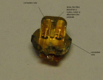
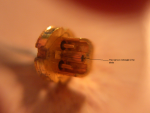
Sun[ch8217]s project will apparently run for five years, in conjunction with Stanford, the University of California, San Diego, and two silicon photonics firms, Luxtera and Kotura. The project builds on previous research done by Sun which attempted to connect chips electrically by stacking them edge to edge. The new method will be based on accurately aligning chips with high precision in order to be able to transmit beams of light across their surface via very narrow channels called wave guides. Basically, every chip would be able to communicate directly with every other chip through a beam of laser light carrying tens billions of bits of data a second. Sun boffins call the new system the [ch8220]macrochip[ch8221], but admit that it has a high risk of failure and is definitely a risk for the company.
A researcher at Sun Laboratories leading the project, Ron Ho, reckons [ch8220]We expect a 50 per cent chance of failure, but if we win we can have as much as a thousand times increase in performance[ch8221]. Researchers also claim that if their idea works, they could finally break Moore[ch8217]s law which states that the number of transistors on a computer chip has to double roughly every two years.
Sun reckons that if the research bears fruit, the project could lead to the manufacturing of smaller computers that were up to a thousand times faster than the ones available today.
yay
i hope they can create it.
how? dont know.. but if it will make our cpu's better, then go ahead.
SUN MICROSYSTEMS has purportedly received a $44 million contract from the Pentagon to explore replacing the wires between computer chips with laser beams. The technology, called silicon photonics, connects chips in such a way that they are able to communicate with each other at incredibly high speeds. If the technology works, it could signal the dawn a new generation of faster, more compact and energy efficient computers.
Semiconductor companies generally produce processor and memory chips by breaking silicon wafers, with thousands of tiny identical circuits etched into them, into pieces. This is supposed to improve manufacturing yields and ensure that a small defect doesn[ch8217]t wreck all the chips.
But now, according to the New York Times, Sun[ch8217]s boffins may have discovered a technique that would be able to do away with the bottleneck data traffic that occurs when information has to be moved around quickly through wires to solve highly complex problems.
[ch8220]Wafer scale integration[ch8221], which involves building bigger chips on a single wafer of silicon, is something that computer scientists have long been suggesting as a technique for developing quicker and faster computers. Silicon Photonics, too, is becoming an increasingly popular field in the Semiconductor firms[ch8217] efforts to replace electrical wiring in processors with optical networking directly built in.
Sun[ch8217]s project will apparently run for five years, in conjunction with Stanford, the University of California, San Diego, and two silicon photonics firms, Luxtera and Kotura. The project builds on previous research done by Sun which attempted to connect chips electrically by stacking them edge to edge. The new method will be based on accurately aligning chips with high precision in order to be able to transmit beams of light across their surface via very narrow channels called wave guides. Basically, every chip would be able to communicate directly with every other chip through a beam of laser light carrying tens billions of bits of data a second. Sun boffins call the new system the [ch8220]macrochip[ch8221], but admit that it has a high risk of failure and is definitely a risk for the company.
A researcher at Sun Laboratories leading the project, Ron Ho, reckons [ch8220]We expect a 50 per cent chance of failure, but if we win we can have as much as a thousand times increase in performance[ch8221]. Researchers also claim that if their idea works, they could finally break Moore[ch8217]s law which states that the number of transistors on a computer chip has to double roughly every two years.
Sun reckons that if the research bears fruit, the project could lead to the manufacturing of smaller computers that were up to a thousand times faster than the ones available today.
yay
i hope they can create it.
how? dont know.. but if it will make our cpu's better, then go ahead.