Welcome to Laser Pointer Forums - discuss green laser pointers, blue laser pointers, and all types of lasers

LPF Donation via Stripe | LPF Donation - Other Methods

Links below open in new window

ArcticMyst Security by Avery

Using a DC/DC converter to power the laser

phenol

0
Joined
Oct 30, 2007
Messages
533
Points
18
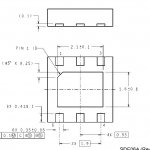
looking at the LLP drawing i noticed that there is a small exposed area of each pad on the sides of the package. i will give it a try there. if it doesnt work, i'l have to borrow some paste from a nearby company /Epiq/ doing chip-on-board mounting and the like
 

Attachments

  • Untitled.jpg
    Untitled.jpg
    42.5 KB · Views: 138


chimo

0
Joined
Jun 20, 2007
Messages
650
Points
0
You could also use a small bit of conductive thermal epoxy for teh bottom pad, however, you would have to very careful not to short the other conductors.
 

IgorT

0
Joined
Oct 24, 2007
Messages
4,177
Points
0
woop said:
thats a lot of power supplies!
i am only worried how to solder the damn thing by hand. i mean how do you heat up under the chip and all the pins at the same time?

It is a lot, yes, but it would be cheap.. At least for the PCBs.. The other components would cost a lot more actually...

I was thinking of ordering the evaluation board, testing it and having my electronics engineer simpy copy it, maybe changing it a little, to make it bigger and allow the use of other inductors, if necessary.


If i should decide to have these PCBs done, they could come with all the components on them already, since i don't think many people would be able to solder this by themselves. This can be done by my company.


Unfortunatelly, the numbers really are big here, when you add in the price of the components... Have to do some calculations, to see how many people would have to be interested, to make it worth it at all.

Don't want to get stuck with 500(?) laser driver PCBs, even if they are cheap..
 

woop

0
Joined
Nov 9, 2007
Messages
342
Points
0
how about a "reflow skillet"
http://www.sparkfun.com/commerce/present.php?p=Reflow Skillet

or a hot air solderer would work as well. anyway its an interesting page
the only thing is, after paying $30 for a hotplate and $30 for solder paste, its not too cheap.

and its not to hard to make your own boards, with a laser printer and some non stick (sticker backing) paper, or commercial paper for the purpose, or photographic boards (which would probably work better for such small pads)
anyway its too easy to justify ordering 500 boards
 
Joined
Dec 13, 2007
Messages
264
Points
0
I have a 500-1000 degree hotair gun, like a hair dryer on steroids. It works well to melt large areas set at 500-600, anything over that and it starts to effect the board. There is a really nice Soldering station on ebay w/ a built in power supply for 180. Shoot, the supply is darn near worth that. It includes everything. Soldering gun, hot air gun w/ nozzles, etc. Nice unit for the $$$. If doing SMD/SMT, this is the only way to go.
Thanks...
 

woop

0
Joined
Nov 9, 2007
Messages
342
Points
0
the samples from national came today... very fast shipping for $8. most stuff off ebay from HK takes weeks. anyway.
that thing is tiny!! i think hot plate reflow might be the way to go. I will lay out a board and see if i can successfully make it and see how i go with solder paste and a hot plate "skillet".
the pads on the side are so small, i don't think they will be much use for soldering by hand
 

Attachments

  • LLP.JPG
    LLP.JPG
    72.1 KB · Views: 136

IgorT

0
Joined
Oct 24, 2007
Messages
4,177
Points
0
Benm said:
If that chip is a 3x3mm LLP, how are the other components going to fit on there? The space for L1 is in the order of 1 x 0.5mm, i doubt any usable inductors come that small.

It turns out, that's not the proper PBC layout for "Design Example 6"..


Here's the link for the demo board datasheet, and it also shows both the top and the bottom layers: http://www.national.com/an/AN/AN-1775.pdf

As you can see, here the IC is so small, it's almost hard to spot, and there is enough place for coils.


Below is what it really looks like.
 

Attachments

  • 3410_Eval_Board.jpg
    3410_Eval_Board.jpg
    24.9 KB · Views: 159

woop

0
Joined
Nov 9, 2007
Messages
342
Points
0
the layout on the datasheet was probably just the general shape and layout of tracks. they probably didn't mean for it to be used. just as a design example.
yeah that board layout makes sense. also notice the holes through the pcb under the chip for heat dissapation
 

IgorT

0
Joined
Oct 24, 2007
Messages
4,177
Points
0
woop said:
the samples from national came today... very fast shipping for $8.

After reading, that you paid for your samples, to come so fast, i thought mine would take weeks, since i didn't pay anything..

But i just came back from the store, and a UPS van was blocking my driveway..

They're here! The 3402 and the 3410!


I can't believe how fast they were.. I only just ordered them.
 

IgorT

0
Joined
Oct 24, 2007
Messages
4,177
Points
0
woop said:
the layout on the datasheet was probably just the general shape and layout of tracks. they probably didn't mean for it to be used. just as a design example.
yeah that board layout makes sense. also notice the holes through the pcb under the chip for heat dissapation
Yes, but the one in the datasheet, did show the layout of the IC itself a lot better.


Anyway, i contacted National about the Evaluation board. If it is available, i will buy it and test it, and if it's good... We'll see.


Oh, BTW: The LM3402 came in a huge sealed bag, with special instructions about humidity outside. Inside was a silica bag, and even a humidity detector card, that shows how long you have to bake the IC. None of the circles were pink, which means, the humidity was well below 10%..

But what worries me, is that the bag itself says, you have only a limited time, to do the baking, after you open it.. WTF? How come these are so much more sensitive. They're much larger, than the 3410. I wonder how seriously i have to take this warning.

I've built many circuits, with lots of different SMD ICs, and i have never gotten such a warning with any of them.
 

woop

0
Joined
Nov 9, 2007
Messages
342
Points
0
I redrew the lm3410 sepec design in eagle. its 23.7mm high 19mm wide and single sided
still learning to use eagle. had to make a new package for the LLP6
what do you guys think?

I might make a larger through hole version fot the diode, caps and resistors. and maybe add a bootstrap circuit to allow operation down to 1.6V to use with 2 AA's
It might be ok just to do away with sepec and make a step up for 2AA rechargable cells 2.4V input and 3V output for a burner.
 

Attachments

  • lm3410_board.JPG
    lm3410_board.JPG
    87.5 KB · Views: 239

woop

0
Joined
Nov 9, 2007
Messages
342
Points
0
and here it is, to scale next to a axiz module

btw; my laser printer prints a lot of stray dots mostly along the sides for some unknown reason. i guess i can't complain, i found it on the side of the road :cool:
 

Attachments

  • nexttolaser.JPG
    nexttolaser.JPG
    55.1 KB · Views: 220

phenol

0
Joined
Oct 30, 2007
Messages
533
Points
18
looks good! it would be best to have the pcb double-sided with 6 -8 vias under the chip in order to use the copper foil on the back as a heatsink. but i guess you cant metallize those vias at home.
 

IgorT

0
Joined
Oct 24, 2007
Messages
4,177
Points
0
woop said:
and here it is, to scale next to a axiz module

btw; my laser printer prints a lot of stray dots mostly along the sides for some unknown reason. i guess i can't complain, i found it on the side of the road   :cool:

That's actualy great!

You didn't need to make any bridge?


I think it would be worth printing it on a better printer tho.. :) Side of the road? :D
 

IgorT

0
Joined
Oct 24, 2007
Messages
4,177
Points
0
phenol said:
looks good! it would be best to have the pcb double-sided with 6 -8 vias under the chip in order to use the copper foil on the back as a heatsink. but i guess you cant metallize those vias at home.

I was just searching for something to make those vias, and there is a device, but it costs 230€ and the tools for different sizes are 90€ each. The smallest one that company makes is 0.4mm, but the smallest one Conrad is selling is 0.6mm dia...


Wouldn't it suffice, to solder some sort of heatsink to the upper ground plane, close to the IC?


Top