Welcome to Laser Pointer Forums - discuss green laser pointers, blue laser pointers, and all types of lasers

LPF Donation via Stripe | LPF Donation - Other Methods

Links below open in new window

ArcticMyst Security by Avery

Multiple Output Boost Driver Design Help. "VLD v1"

ki4mor

New member
Joined
Apr 20, 2021
Messages
1
Points
1
Hello Everyone, First post so take it easy :).

Driver Design Intent:

I have long wondered why we don't see drivers that can change output like most modern flashlights. I really like the idea of being able to use my 100+mw laser pointer for less blinding tasks. I have since embarked on crashing the 2 worlds of LPF and BLF together.

Design:

I have started a design based on the Benboost Mini using a LM3140, then added a Attiny13a microcontroller to deal with the PWM control on the Dim pin of the LM3410. Thanks to some very intelligent and generous members of the Flashlight Community. I managed to find, then tweak some .c code to change a PWM signal every time the power cycled with a tail switch.

Everything worked great when I was proving this design on a breadboard, so I went ahead and get to work on a PCB. I figured why not use a Flashlight host to house this, as they are readily available in a multitude battery configurations. So got a few 18mm boards made and get everything soldered up.

Issues:

I am not well versed in EE or PCB Design and have basically stubbled though this which brings me to asking for help. I cannot seam to get consistent function out of the microcontroller when it is attached to the PCB. I have a few theories based on complete guesses. Maybe drawing power direct from the same leg as the inductor might be sending unwanted voltage spikes to the MCU?

Summary:

I have added the schematic and PCB design as it stands with a project name of "VLD" (or Variable Laser Driver). In its current state v1 is semi functional. As in powers a test load and laser diode but the mode cycling is just random. I hope that some members with more experience in driver design and an interest in adapting multimode operation like the Flashlight community might have some insight into possible upgrades to the current design. I have this in an EasyEDA project too and would love to share with the community in whatever way would be easiest.

If you made it this far thanks for reading.
 

Attachments

  • Bottom.png
    Bottom.png
    67.2 KB · Views: 11
  • Schematic.png
    Schematic.png
    124.4 KB · Views: 13
  • Top.png
    Top.png
    82.9 KB · Views: 11


Giannis_TDM

Well-known member
Joined
Apr 27, 2019
Messages
895
Points
93
Hello Everyone, First post so take it easy :).

Driver Design Intent:

I have long wondered why we don't see drivers that can change output like most modern flashlights. I really like the idea of being able to use my 100+mw laser pointer for less blinding tasks. I have since embarked on crashing the 2 worlds of LPF and BLF together.

Design:

I have started a design based on the Benboost Mini using a LM3140, then added a Attiny13a microcontroller to deal with the PWM control on the Dim pin of the LM3410. Thanks to some very intelligent and generous members of the Flashlight Community. I managed to find, then tweak some .c code to change a PWM signal every time the power cycled with a tail switch.

Everything worked great when I was proving this design on a breadboard, so I went ahead and get to work on a PCB. I figured why not use a Flashlight host to house this, as they are readily available in a multitude battery configurations. So got a few 18mm boards made and get everything soldered up.

Issues:

I am not well versed in EE or PCB Design and have basically stubbled though this which brings me to asking for help. I cannot seam to get consistent function out of the microcontroller when it is attached to the PCB. I have a few theories based on complete guesses. Maybe drawing power direct from the same leg as the inductor might be sending unwanted voltage spikes to the MCU?

Summary:

I have added the schematic and PCB design as it stands with a project name of "VLD" (or Variable Laser Driver). In its current state v1 is semi functional. As in powers a test load and laser diode but the mode cycling is just random. I hope that some members with more experience in driver design and an interest in adapting multimode operation like the Flashlight community might have some insight into possible upgrades to the current design. I have this in an EasyEDA project too and would love to share with the community in whatever way would be easiest.

If you made it this far thanks for reading.
You have most likely killed your microprocessor or at least caused it to fall into an off state per say, If you want to power it that way you must use an LDO set to whatever the MC needs powered from the battery, Not the output inductor( this(powering the MC from the inductor before the rectifying diode) will aIso have the side effect of completely fucking the current limiting so do what I told you and power it with an LDO from the battery) can give some advice on PCB and schematic design. For instance, switch to kicad Easyeda is not good at all. And some other issues I can see off the bat: The rect diode is on the wrong side of the inductor, The inductor SW node is too large in length and will cause lots of noise and the layout is not that good to say the least. Hit me up on either LPF PMs or discord to arrange a vc in which Ill teach you basic layout and general SMPS PCB design guidelines.
 

farbe2

Well-known member
Joined
Oct 3, 2018
Messages
303
Points
63
I don't see a problem with powering the uC from this node, if you stay within the data sheet limits.
If you use a uC thats rated 1,8->5V it would be perfectly reasonable to power it directly from a single 18650 cell.
However your mistake is likely that you dont have any (working) bypass caps on the uC (and the sepic driver).
Your switcher will short the inductor to ground to charge it. This will take massive amounts of currents for a short period of time. These current make your voltage drop (because of resistance). This could easily cause your uC to detect a brownout and switch off or get stuck if you dont have your BOD enabled.

The "big" input capacitor C6 should supply the current, however it can only do that if its really close (physically) to the load e.g. the sepic IC.
Look how long the leads are for the complete loop C6 -> inductor -> switcher -> ground -> C6. You want this loop to be as small as possible. This will result in more current drawn from C6, so less voltage drop.
The "loop area" is also important for noise reduction. If your loop area is big, big magnetic fields will be created. If there is something inside the loop or close to it, it will get influenced.
So make shure your uC is not inside the danger zone.

However a trap for young players: also look at the loop area and length for discharging (inductor -> diode -> c4/5 -> GND -> C6) this also matters for radiation and pulse currents.
If your charge loop is good but your discharge loop sucks, it could introduce current, therefor voltage drop, in your ground. This would jackup your voltage at a different load.(that uses the same ground as C4/5 for example)

Also use a bypass cap very close to the uC, the uC also draws puls current synchronized to the clock. These currents are typically very short and high, resulting in resistive and! inductive voltage drop. Remember each wire is also a inductor and a inductor will have a impedance (think frequency depended resistance) that rises with the frequency. So short (high frequency) current draw will cause more voltage drop than steady state current draw because of the impedance.
 

Giannis_TDM

Well-known member
Joined
Apr 27, 2019
Messages
895
Points
93
I don't see a problem with powering the uC from this node, if you stay within the data sheet limits.
If you use a uC thats rated 1,8->5V it would be perfectly reasonable to power it directly from a single 18650 cell.
However your mistake is likely that you dont have any (working) bypass caps on the uC (and the sepic driver).
Your switcher will short the inductor to ground to charge it. This will take massive amounts of currents for a short period of time. These current make your voltage drop (because of resistance). This could easily cause your uC to detect a brownout and switch off or get stuck if you dont have your BOD enabled.

The "big" input capacitor C6 should supply the current, however it can only do that if its really close (physically) to the load e.g. the sepic IC.
Look how long the leads are for the complete loop C6 -> inductor -> switcher -> ground -> C6. You want this loop to be as small as possible. This will result in more current drawn from C6, so less voltage drop.
The "loop area" is also important for noise reduction. If your loop area is big, big magnetic fields will be created. If there is something inside the loop or close to it, it will get influenced.
So make shure your uC is not inside the danger zone.

However a trap for young players: also look at the loop area and length for discharging (inductor -> diode -> c4/5 -> GND -> C6) this also matters for radiation and pulse currents.
If your charge loop is good but your discharge loop sucks, it could introduce current, therefor voltage drop, in your ground. This would jackup your voltage at a different load.(that uses the same ground as C4/5 for example)

Also use a bypass cap very close to the uC, the uC also draws puls current synchronized to the clock. These currents are typically very short and high, resulting in resistive and! inductive voltage drop. Remember each wire is also a inductor and a inductor will have a impedance (think frequency depended resistance) that rises with the frequency. So short (high frequency) current draw will cause more voltage drop than steady state current draw because of the impedance.
Think for a second, The IC isnt even switching properly here cause the diode and output cap net is on the wrong side of the inductor(the SW side) Causing the battery voltage every time the IC tries to switch to pass through them to charge the caps. Lets say he fixes that, Another HUGE problem is that if he powers the uC from that node that you said is acceptable the uC would instantly get killed due to the vin to it reaching ~28v( that's what happens since we are currently limiting here, Laser diodes consume ~150mA For the power he mentioned that he wants to reach whilst the uC will want barely a mA so the boost converter will just keep raising the voltage till the set current of ~150mA passes through it hence it will reach 28v ish and kill it. Might I also point out that this will somewhat fuck with the current limiting due to the uC drawing current as well as the LD.
 

farbe2

Well-known member
Joined
Oct 3, 2018
Messages
303
Points
63
I don't think you understand that circuit.
The LM3410 is a boost driver, so the circuit around it (switch node connected to diode) is clearly right.
Just look inside the data sheet.
The uC is also not powered by the output of the converter. Its clearly powered by the input. Pin5 is the voltage input pin of the LM3410. C6 the input capacitor. This voltage comes form the terminals V+ and V- (YEET / BAT-). It only gets passed through if the polarization is correct because of Q2. I would have used a N-ch get because of lower losses, but this is ok too.

So all you claims that it kills the uC are false because the uC is not connected to the Switcher output.
I don't blame you, the circuit is not drawn good.
Thats also a trap for young players: Drawing you circuit good helps immensely for understanding its function.
Some simple rules are:
Keep ground symboles on the bottom oriented the right way.
Make your power/signal flow from left to right and top to bottom.
Make functional blocks and use labels, for example make the Input protection a block and name the output accordingly. Don't draw lines for supply voltages all over the place. Use multiple labels.
This is not really a problem for small circuits, however if you get into circuits that use >1000 components its a big issue.


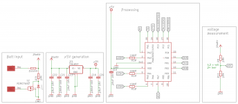
Have a look at one of my circuits. Its not the whole schematics but it shows the principle of using "design blocks".
It also helps to place the bypass capacitors in their block, for example C15 is bypassing the uC, C16 on the other hand is for stabilizing the linear regulator. Both are connected to 5V and GND, but they do different stuff inside the circuit as indicated by the schematic.

Bildschirmfoto 2021-05-18 um 12.44.04.png
 

Giannis_TDM

Well-known member
Joined
Apr 27, 2019
Messages
895
Points
93
OTE="farbe2, post: 1601608, member: 56105"]
I don't think you understand that circuit.
The LM3410 is a boost driver, so the circuit around it (switch node connected to diode) is clearly right.
Just look inside the data sheet.
The uC is also not powered by the output of the converter. Its clearly powered by the input. Pin5 is the voltage input pin of the LM3410. C6 the input capacitor. This voltage comes form the terminals V+ and V- (YEET / BAT-). It only gets passed through if the polarization is correct because of Q2. I would have used a N-ch get because of lower losses, but this is ok too.

So all you claims that it kills the uC are false because the uC is not connected to the Switcher output.
I don't blame you, the circuit is not drawn good.
Thats also a trap for young players: Drawing you circuit good helps immensely for understanding its function.
Some simple rules are:
Keep ground symboles on the bottom oriented the right way.
Make your power/signal flow from left to right and top to bottom.
Make functional blocks and use labels, for example make the Input protection a block and name the output accordingly. Don't draw lines for supply voltages all over the place. Use multiple labels.
This is not really a problem for small circuits, however if you get into circuits that use >1000 components its a big issue.


Have a look at one of my circuits. Its not the whole schematics but it shows the principle of using "design blocks".
It also helps to place the bypass capacitors in their block, for example C15 is bypassing the uC, C16 on the other hand is for stabilizing the linear regulator. Both are connected to 5V and GND, but they do different stuff inside the circuit as indicated by the schematic.

View attachment 72727
[/QUOTE]
You are in fact correct, just noticed that his bottom layer is mirrored at 180 degrees for some reason.. and yup that's how I do my schematics too


Top