- Joined
- Sep 12, 2007
- Messages
- 9,399
- Points
- 113


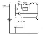
I don't see why the inversion is necessary. Why not just flip the cell and put the switching and sense elements "after" the load?
Something like this crude paint sketch:

(BJTs are easier to draw than FETs)
The challenge with that IC is that it disrupts the common (+). The AMC doesn't, which is why it works well here. I can't see a way to make that Linear chip common positive.

I don't see why the inversion is necessary. Why not just flip the cell and put the switching and sense elements "after" the load?
Something like this crude paint sketch:
(BJTs are easier to draw than FETs
An open drain P channel driving the gate of an N mos is not ideal due to not enough pull down current capability.
You could rig a boost controller IC in buck mode with the negative side switched rather than the positive supply.
This wouldn't work?


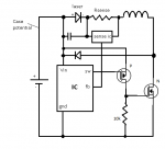
Something like this gate drive idea should work. Just switch the PNP and NPN for inversion.
Something like this gate drive idea should work. Just switch the PNP and NPN for inversion.
I have used that before. Very fast and very
effective
Cyparagon / TLS, What do you think of this part, to accomplish the inversion above?
- Rohm QSZ2TR http://rohmfs.rohm.com/en/products/databook/datasheet/discrete/transistor/bipolar/qsz2.pdf
and is there need for the 560 and 22 ohm resistors shown?
The flyback driver example just amplifies the gate drive; it doesn't invert it. That device won't invert the gate drive either. The BJTs have common collectors, and need to be either separate, or have common emitters.
22 probably isn't necessary, but 560 is certainly needed to limit the base current. The IC's gate drive is basically powering a short without that. It may also need to be higher or lower, depending on what sort of gate current the switching IC can typically handle.
Seems like the 560 should be lower. IC can typically handle 500mA gate current.