Welcome to Laser Pointer Forums - discuss green laser pointers, blue laser pointers, and all types of lasers

LPF Donation via Stripe | LPF Donation - Other Methods

Links below open in new window

ArcticMyst Security by Avery

Experimental BB-D Driver (Open Source)

Hiemal

0
Joined
Dec 27, 2011
Messages
1,443
Points
63
Hey guys.

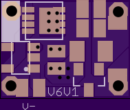
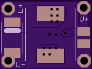
So I wanted to share with you all a new driver design I came up with based off of a schematic I found in an OnSemi datasheet.

http://www.onsemi.com/pub_link/Collateral/MC34166-D.PDF

If you scroll down to page 10, you'll see the schematic I speak of.

The addition of an extra mosfet and diode seems to allow you to add the ability for any bucking regulator to boost as well, in effect creating a buck boost regulator. The greatest plus of using this method vs a true buck boost regulator is the ease of sourcing for bucking regulators, and the improved voltage capabilities/current capabilities that typically come with them.

Can you say max 18 volts input + 3 amps of potential output current?


I've done a great deal of looking around at different parts and whatnot to see what could potentially fit this bill properly, and I found these.

ST1S10PHR STMicroelectronics | Mouser

Si2338DS-T1-GE3 Vishay Semiconductors | Mouser

SK44BL-TP Micro Commercial Components (MCC) | Mouser

Basically I followed the schematic on the Onsemi sheet, and also followed the ST1S10PHR's schematic as well and came up with this design. The ST1S10PHR I chose for price, and the fact that it's a synchronous bucking converter meaning it doesn't require another schottky diode for rectification.

2cKmQ08.png


One of the biggest obvious downsides to the addition of more parts is a slight efficiency loss.


Parts List

1 x ZXCT1109

1 x ST1S10PHR

1 x SI2338DS-T1-GE3

2 x 10 uF 0603 package capacitor

1 x 10 uF 0805 package capacitor (you can swap these two as necessary)

1 x potentiometer (have to decide if it's going to be 47k or 10k...)

1 x sense resistor (again the exact value has yet to be determined, around 0.025-0.05 ohms)

1 x 1k ohm resistor 0603


The inductor used could be this one
http://www.mouser.com/ProductDetail...GAEpiMZZMsg%2by3WlYCkU5iuzh4MJmq0m6sYdqgpoaI=

Or this, with slightly higher inductance but slightly lower current rating.
http://www.mouser.com/ProductDetail...EpiMZZMsg%2by3WlYCkU5iuzh4MJmq06IRHC1l%2bnhU=


I'm releasing it as open source, since this is highly experimental and I'd love for anyone who has experience with this sort of thing to give a hand since it's quite different.
 
Last edited:


rhd

0
Joined
Dec 7, 2010
Messages
8,475
Points
0
SXeyqq7.png

and here's the schematic

I love this initiative!

Here are my thoughts:

1) I don't think your current sensing setup will work. This is an attempt at an inverted buck topology. As weird as it is to think this way, your GND2 actually becomes the LD+, and what you've got labelled as LDOUT, becomes the LD-. This means that the way you've got it setup now, you're basically trying to do low side monitoring, with ZXCT backwards. Even if it worked, the ZXCT would be trying to generate a feedback voltage that is lower than the IC's GND (lower, by at least the VDrop of the LD). It's the inverted buck topology that complicates things. Luckily, we don't really care that it's inverted, since input and output are totally isolated, but it does make current sensing a bit more complicated.

Current sensing becomes the annoying head scratcher. The solution may be to find a current sense monitor that is meant for taking measurements isolated from the output circuitry itself, and that takes independent power from VIN. I believe such things exist. If you can power the sense monitor from VIN, and generate a feedback voltage from a sense resistor on the actual high side of the inverted output (which would basically mean a sense resistor right before "GND2" on your schematic, I think that *might* work, as long as it creates the feedback voltage relative to the IC's GND.

Again, headscratching here.

2) Aren't you missing a second diode that should be somewhere between the SW pin and the inductor?

3) 3A of switch current, in a boost driver, isn't enough to do much with. For true consistent 2.4A 5.2V output from a boost, you need more like 4.5A+ of switch current.

4) Going with an IC that has an internal switch seems like a waste all-together. It's not future proof. You're tying a lot of design work to an IC that can't scale. I initially used buck ICs with internal switches, but eventually designed a circuit around one that used an external MOSFET, and now I have a base circuit that I've used for everything from sensitive 100mA LDs, to beefy 15A LED flashlights. So I would suggest grabbing a different IC. If you PM me, I'll tell you what my favourite superhero buck IC is. If you think you can adapt it into a boost-buck (and will share back), I'll even send you some buck SCH / BRD files to jump in with.
 
Last edited:

Hiemal

0
Joined
Dec 27, 2011
Messages
1,443
Points
63
I love this initiative!

Here are my thoughts:

1) I don't think your current sensing setup will work. This is an attempt at an inverted buck topology.

I don't think it is actually inverting; I took another look just to make sure at the ONsemi schematic and the way the capacitor is laid out on the output, it's definitely non-inverting. On Page 11 there IS an inverting version with a lower part count but for the sake of continuous ground, and ease of use I'm thinking this method is probably better.

And current sensing actually shouldn't be too difficult if you went with inverting. You'd just have to swap the ZXCT's sense pins around. It wouldn't know the difference and would actually simplify the current sensing completely since the output of the ZXCT should still be positive.

2) Aren't you missing a second diode that should be somewhere between the SW pin and the inductor?

Nope, it's a synchronous buck converter. This means there's another mosfet that's inside of the main IC that does the rectification for you for higher efficiency and lower part count. No external one needed!

3) 3A of switch current, in a boost driver, isn't enough to do much with. For true consistent 2.4A 5.2V output from a boost, you need more like 4.5A+ of switch current.

Actually, the 3 amps is a constant current measurement when bucking. The actual switch current rating is a whopping 5 amps.

4) Going with an IC that has an internal switch seems like a waste all-together.

It depends on how you look at it. Internal switch IC's definitely save a LOT of board space (esp with the synchronous part too). I mean, if I went with an external switch IC, I'd have two mosfets, and two diodes to shove on the board somewhere, PLUS the main IC, PLUS the current sense op amp.

It'd be a lot to fit, and while yes it very likely would give a greater degree of flexibility I'm really liking the space saving of this chip while still being in a relatively large, easy to use package (memories of trying to solder QFN packages haunt me to this day)
 
Last edited:

rhd

0
Joined
Dec 7, 2010
Messages
8,475
Points
0
I don't think it is actually inverting; I took another look just to make sure at the ONsemi schematic and the way the capacitor is laid out on the output, it's definitely non-inverting. On Page 11 there IS an inverting version with a lower part count but for the sake of continuous ground, and ease of use I'm thinking this method is probably better.

(...)

It depends on how you look at it. Internal switch IC's definitely save a LOT of board space (esp with the synchronous part too). I mean, if I went with an external switch IC, I'd have two mosfets, and two diodes to shove on the board somewhere, PLUS the main IC, PLUS the current sense op amp.

It'd be a lot to fit, and while yes it very likely would give a greater degree of flexibility I'm really liking the space saving of this chip while still being in a relatively large, easy to use package (memories of trying to solder QFN packages haunt me to this day)

Interesting - I think you're right re: the non-inversion. That's really handy, and in that case, resolves my comment re: current sensing being an issue (though I maintain that with inversion, it still would be).

I don't think the external mosfet route should scare you off though. They're tiny. Here's a 4.5A buck I just did, using an external MOSFET, and the whole thing fits on a cozy 9x12 mm (FlexDrive size). Adding a second MOSFET wouldn't be that much of a challenge.

i.png


i.png
 
Last edited:

Hiemal

0
Joined
Dec 27, 2011
Messages
1,443
Points
63
A second mosfet and a second diode, too, since external mosfet buck controllers can't technically be synchronous.

If I tried to make an external mosfet buck boost, I think I would actually attempt the inverting schematic for it. It seems like it would be better fit for it somehow.
 

Hiemal

0
Joined
Dec 27, 2011
Messages
1,443
Points
63
Some updates, also discussed in my driver thread:

It does seem to kind of work. Bucking it behaves as it should, regulating properly but producing more heat than it should given the output currents.

Boosting it just does not seem capable of doing without producing an audible squeal and the output seems to be a pulse of sorts, in the audio frequency range and ridiculous amounts of heat. I'm unsure if this is a heat related issue, or if it's some sort of protection that's kicking in on the driver. Either way the heat it's producing does NOT make sense given the output current, so I'm unsure where to go with this. Additionally the driver's board design actually has a minor error which I've fixed in a new version of the driver board.
 
Joined
Sep 22, 2015
Messages
1
Points
0
The information you shared here is very helpful. Thanks for sharing it with us. I want to know more about your Buck and Boost converters and their designing. What output you are getting from it ? Are they working efficiently? Please explain with the circuit if you can.
 
Last edited:


Top