Welcome to Laser Pointer Forums - discuss green laser pointers, blue laser pointers, and all types of lasers

LPF Donation via Stripe | LPF Donation - Other Methods

Links below open in new window

ArcticMyst Security by Avery

Diode damage?

rvrh3

0
Joined
Nov 18, 2010
Messages
129
Points
28
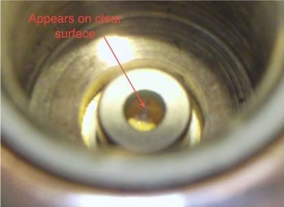
I know there has already been threads about the phantom square that appears from a 445nm diodes and that its normal. I got one of Yobresal's builds. The issue is that I don't remember this particular square to have been there when I first received this laser, and upon inspection I found a small line on the clear opening of the diode itself. Im wondering if anyone thinks this might be where the "phantom" square comes from...

This is the best closeup image of the small line that I could take with my camera.
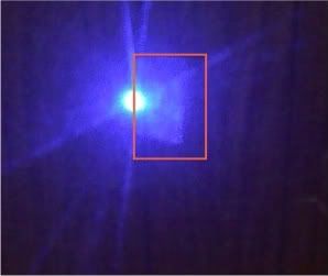
445nmdiode-1-1.jpg


Here is the square.
phantomsquare.jpg


If it is something on the surface of the diode "window" (don't know the proper term) What would be the best way to try to clean it? (That is, if it can be cleaned)

Thanks in advance!

-Rob


GBD

0
Joined
Oct 25, 2010
Messages
783
Points
0
Window is the correct term.

Alot of diodes have this artifact and impression on the window, and it isn't cleanable, it looks like its burned onto the AR coating.

I would say don't worry about it, all my 445nm's have a simular appearance.

As for the square, it could be caused by your collimating lens, but I doubt your diode's window has anything to do with it. (So clean the lens, but don't touch the diode's window, looks like nothings wrong with it.)
 
Last edited:
Joined
May 4, 2009
Messages
5,443
Points
113
Yes GBD is correct there as I have seen lit 100's of these diodes and every one has that faint streak across the window.
I don't think this is what is giving you the squair you speak about though.
it is most likely comming from the die it's self, clean your lens and if it stays there then it's the laser die.
 
Last edited:
Joined
May 25, 2010
Messages
3,655
Points
0
That square is in every 445nm diode i own have seen. Nothing to worry about.

It is not the diode window. I have a De canned 445nm diode and it has the square.;)
 
Last edited:
Joined
Sep 16, 2007
Messages
3,658
Points
113
I noticed the "mark" on the diode window with 445s and 405s at high power. With the 445s, the mark is more of a line. With the 405s, the mark is more elliptical which corresponds to the beam profile of the diode.

I would deduce that the mark on the diode window is a deposit of vaporized particulate that is trapped between the diode can and the lens. I have successfully cleaned it with some alcohol, a cotton swab or two, and gentle pressure.
In my experience, the spot/streak/whatever on the window does not affect the beam except for a small power loss.* No noticeable beam artifacts were caused by this.
Immediately after installation of these 445nm diodes, I clean the "spot" off the window as it seems that this mark is burned onto the window (possibly during QC checks) even before I power up the diode for the first time. I never noticed the mark on the window of diodes set to output lower powers (~150mW).

If you want to keep the diode window clean, it helps to seal the lens with some teflon tape and avoid turning the lens to focus the beam so much. Using the laser in humid or dusty environments may contribute to this mark on the window.

*I measured power before and after cleaning the window of a stable 405nm - with the dirty window, power was ~476mW. After it was 480mW spot on where it was supposed to be.
 
Joined
Apr 16, 2011
Messages
2
Points
0
I have the same problem with my 1,2W O-like blue laser. Here is my photos.
 

Attachments

  • Diod01.jpg
    Diod01.jpg
    137.6 KB · Views: 298
  • Resize of Resize of IMG_9337.JPG
    Resize of Resize of IMG_9337.JPG
    35 KB · Views: 264
  • Resize of Diod02.jpg
    Resize of Diod02.jpg
    74.5 KB · Views: 230


Top