Welcome to Laser Pointer Forums - discuss green laser pointers, blue laser pointers, and all types of lasers

LPF Donation via Stripe | LPF Donation - Other Methods

Links below open in new window

ArcticMyst Security by Avery

Tesla Coil Build Thread

Joined
Dec 14, 2008
Messages
33
Points
18
To embed YT video's use ..
And yes in the last video you can easily see the energy being ramped, instead of dumped...a clear rise and fall. Clever design.

Thanks. In fact a similar effect can be achieved the same way VTTCs do so, by using the rising sine wave of the mains to drive a small SSTC.

14625415292_471d4cefca_c.jpg


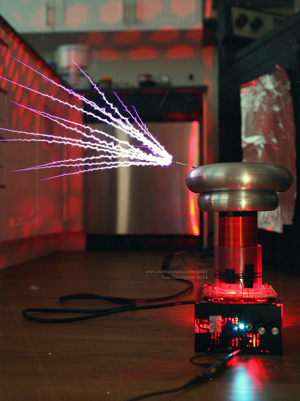
This was designed primarily to experiment with this effect before moving on to the more complex QCW designs. It was also an exercise in developing a single board SSTC just for fun, of which I recently updated to use a full bridge of IGBTs:

24756445355_cac58883e6_c.jpg


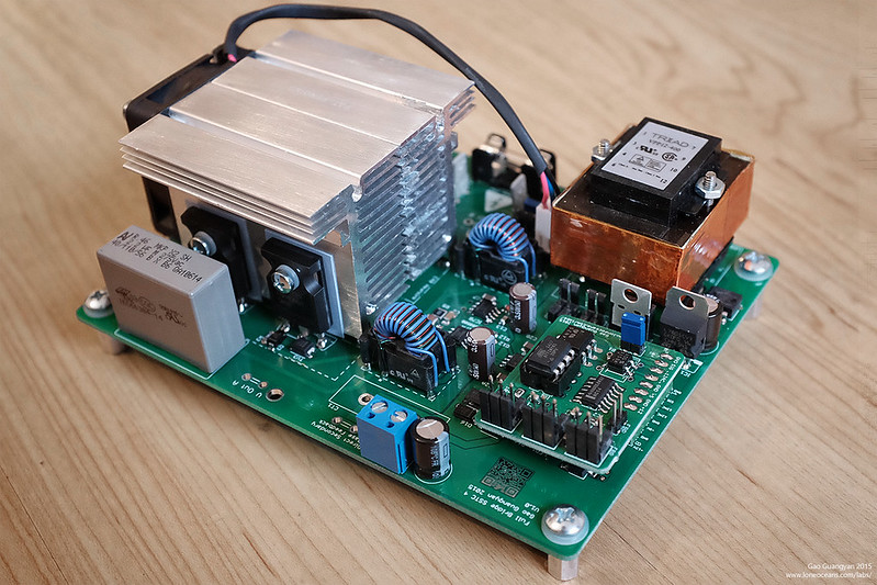
This was designed to fit into most ATX power supply boxes (not an ideal choice I know! But it makes for a cute case!), and also features swappable interrupter cards just like a graphics card on a motherboard. So far it's been a nice little design which I use to test some new ideas since it was designed to be a relatively simple general purpose SSTC platform. :)
 
Last edited:


Joined
Aug 16, 2013
Messages
971
Points
43
Hey, I just have a question for some of you veterans, I think I'm having a problem with component heat transfer. I understand this might be some what obvious but is melting on the thermal tabs a sign that there is poor heat transfer or does it represent another aspect of component failure.
Physically the diodes and fets appear normal but fail common fet and diode tests.


These of course are trash but I think once one failed it started a cascade effect. The coil worked great for 2 weeks until one day after a duty cycle longer then usual the coil just quit. The AL heat sink was barely warm.
To rectify this I ordered new fets and diode's with a much thinner sil-pad. Wish me luck. Bridge rebuild #5.
 
Joined
Dec 14, 2008
Messages
33
Points
18
Hey, I just have a question for some of you veterans, I think I'm having a problem with component heat transfer. I understand this might be some what obvious but is melting on the thermal tabs a sign that there is poor heat transfer or does it represent another aspect of component failure.
Physically the diodes and fets appear normal but fail common fet and diode tests.


These of course are trash but I think once one failed it started a cascade effect. The coil worked great for 2 weeks until one day after a duty cycle longer then usual the coil just quit. The AL heat sink was barely warm.
To rectify this I ordered new fets and diode's with a much thinner sil-pad. Wish me luck. Bridge rebuild #5.


DownWithUmbrella,

That looks like pretty bad heating on the components!.. and it even looks like the tinning on the metal surfaces has melted, meaning that the components have got really hot. So suppose they were heat sunk to the heat sink with a sil-pad? If so this means either your heat-sinking is severely lacking, or you're getting a lot of losses really quickly in the components.

What sort of setup were you running and what sort of duty cycle? Do you have other parameters such as primary current? Also, what frequency is your SSTC running at?

One thing that jumped out to me was that you were using some really big TO264 transistors + separate diodes. What was the reason for this choice? I'm not sure how big your setup is but it looks like an unnecessarily large bridge unless you're driving a -really- large coil, and you'll also need a very robust gate driver. What gate drive voltage and resistors are you using and which gate driver? It's also possible that the FET is not getting into saturation (or high enough saturation) leading to high conduction losses. Even the good old IRFP260/460 should be good enough for a big 1+kW CW coil.

Seeing that this is your 5th bridge, if they all have similar failures, I'll probably try to do something different. Simply replacing components will not be solving your problem and you'll just end up with the same thing. Certainly it looks like your entire setup needs significantly better cooling since it appears that your sink is barely warm yet your components must have got blisteringly hot.

Overall I'd check for:

1. Proper heat-sinking setup. Do you have a photo? One possible option is to ditch the silpad and use separate small heatsinks per switch.

2. High inductance bus and wiring - will cause excessive losses = heat + switch / diode failure. It looks like your components all have long legs meaning they were probably connected with soldered wires? This isn't an ideal setup, probably a good idea to make some sort of laminated PCB or keep your wire loops as small as possible, though I guess that's difficult without a double layer PCB.

3. Is your driver up to task? - what driver are you using? What MOSFET switch are you using? Is is necessary to use such a big Fet?

4. Redundant Diode - good FETs have optimized body diodes these days, adding external diodes may not be required and may be detrimental for a variety of reasons.. in this case it looks like those diodes are very unhappy!

5. Consider perhaps IGBTs - they may be suitable for your use and typically have excellent co-pack diodes, and prices are very good these days!

6. Resonant frequency - may be excessively high - increase switching losses

7. Gate Drive voltage - too high a frequency can cause your gate drive voltage to drop especially if your driver / power supply is not up to it, leaving your switches in sub-saturation

8. GDT - I assume you're using a GDT - is the GDT the right material? Have you scoped the gate voltage during operation?

9. Finally, maybe also try lowering your duty cycle with an interrupter - I presume you're running near CW to get these kinds of heating on the TO264/220 tabs!

Overall for this kind of heating to occur my immediate guess is insufficient gate drive of the switches as the biggest problem + insufficient sinking and high duty cycle.

Need to have it on hand to investigate properly though since I'm just making wild guesses but good luck!
 
Last edited:
Joined
Dec 11, 2011
Messages
4,364
Points
83
I think it all came down to the silpad he was using since it was (I think) excessively thick and of poor thermal impedance (high).

Isolated individual heatsinks would be best but I don't think it's an option for him. He's had heatsink isolation issues since bridge 1.0, resulting in most/all of the previous failures.

IIRC he's running a >1.3kW CW single resonant coil off of 340Vbus at >200KHz. I'd have to dig through emails but I'm sure he can answer specifics better. He's using my overall designs, though there will be layout differences in his iteration for sure. I have body diode blocking and bypassing diodes in my build because I found that if ever driven into the capacitive region the commutation through the body diode would cause failures when running CW. I haven't had a single FET fail in my iterations based on this design so far.

Hopefully the new silpads do the trick!
 
Joined
Aug 16, 2013
Messages
971
Points
43
Here are two photos of my bridge. By just looking at the bridge this should answer some of your questions. The bridge is free standing but my next one will be a PCB board lay out.
I'm willing to say 95% of this coil is based off Sigurthr's design. With that said I have done all the physical construction (or destruction).
I am using the USSSTC driver(are you familiar). The coil runs CW right now because I don't have the kit yet for the interrupter.

From the variac to the bridge I have a voltage doubler 344VDC. The coil did run fine with or without it. Pulling 16A and 12A respectively. With the doubler and the variac at 100% the coil had an out out of 1.3kW. Without the doubler it peaked around 850-900Watts. For two weeks I was awe struck by how amazing a 1.3kW SSTC was! Then one day after about 4-5 mins of 60% power. It simply shut down. I replaced a fet. It fired up for a second then donezo.

The the goal was initially 900w but of course once I got close I only wanted to go bigger.
Early failures I think were due to mounting issues. I'm using conductive hardware. Now I've mitigated that.
When I set up the Oscope I read a resonate frequency of 222kHz. I have not scoped the GDT. Only to verify my phasing.

I'm not sure why sig included the body isolation diodes. Added protection?

The photos don't do it perfect justice. It is soldered solidly with plent of Arctic 5 grease. The padding Is a sheet of sil-pad. The HS is massive and the copper plate was put there to layer the components for ease of soldering. It might be more trouble then it's worth.

Adding to the bad news I bought a small bridge that worked with the coil to begin with from sig. Today that doesn't work either which hints to driver failure but nothing obvious seems damaged.
I really really enjoy TCs but my skill might just not be up to par.


I know running the coil full blast in CW mode is demanding but nothing seem to ever get hot?? That was when I was using a thick elastic polymer as a pad. Worked great. Now nothing.
I really appreciate your patience here on the thread, everyone's talking about crazy coils like you build loneocean and I'm still stuck on SSTCs. This is the last one:/

As it sits right now I don't even know where to start. Nothing works. The current half bridge as I rebuilt it last night SHOULD work as it is identical minus the sil-pad swap + all new components. I DONT think this bridge is dead. Something else could be the issue. Oscillation has always initiated so I don't think it's that. Next maybe trouble shoot the driver ?
 
Last edited:
Joined
Dec 11, 2011
Messages
4,364
Points
83
Yep time to look at the driver. I'd wager the UCC chips might have gotten backlash and given up the goat. Disconnect the GDT from the driver, scope the output of the driver, touch the antenna with your finger to inject mains hum and you should see a nice waveform out. If there's not enough mains hum you can use a 555 timer or some-such (you can even use an audio signal, just play a sine/square wave etc).

If you only get positive or negative pulses it will look like +-6V because of the dc-blocking cap, this indicates a single UCC chip has failed. If you get no output, it's likely both have failed OR the schmitt trigger failed (I've never seen this happen, but it's possible). If you get +-12V pulses all chips are fine.

P.s. I recently tested my GDT cores in HF radio use; they're good well past 4MHz!
 
Joined
May 30, 2011
Messages
218
Points
18
Hey, I finished my SSTC build and have been testing it at 12V. I was wondering if anyone has any experience with arcing at the bottom of the secondary?

The bottom of the secondary is only connected to the strike ring.

The only arcing I am seeing is from the bottom between the wire connecting the bottom of the secondary to the strike ring. I can't run it too long like this because it just ends up melting the wire.

I am under the assumption that it is because my grounding is non-existent? Just wanted to make sure there were not any other solutions to this problem other than a connection to RF ground.
 

Pman

0
Joined
Nov 28, 2012
Messages
4,447
Points
113
:( :( :( Wish I understood all of this. It's really beautiful. I honestly feel too old and tired to learn it to be.completely honest. All the years of pain meds have taken their toll. Its not at all that I couldn't, it's that I just don't have the energy. Just being honest. Not like I wouldn't love to own one though. Haven't seen anything this live since grade school I think. I'll look into some kits though. Is there anything worthwhile out there that isn't too expensive that is actually recommendable? Probably way better off buying one who built it themselves.
 
Joined
Dec 14, 2008
Messages
33
Points
18
Down with Umbrella,

Thanks for sharing the details. Here’s a very quick reply for now but let’s try to break this down into two aspects – (1) Physical construction and heatsinking, and (2) Electronics.

Physical Construction

That looks like an ok set-up you got there. Ideally I’d try to tidy it up even further but keeping all connections as short as possible. For example I typically bend the leads and form them into nice tidy shapes, carefully solder them, and cut the excess away. You also seem to be using pretty thick wire which is typically difficult to physically hold it place – I’d recommend just using slightly thinner wire locally before branching off to larger wires later but not a big deal.

Second, not quite sure how the heat-sinking is working and I’m not sure why you have that additional copper plate there? If you don’t thermally bond the copper and aluminium properly it seems to be more trouble than simply just bolting the transistors to the aluminium sink with the thermal pad. It looks like two of the TO220 packages are clamped by the tab with some plastic to the thermal pad - you have the right idea and it’s a good way to mount, but this can be better done by mounting a stiffer bar made of metal (typically a C-section bar is used) pressing the TO220 right in the middle.

Articl01thermal.jpg

The setup can be something like in the photo above though note that that could be improved (see the gap!). Likewise with your free-floating TO220 packages. Make sure all your mounting screws are also tightened appropriately and that you choose a good silpad. What you have looks ok though so I’m still surprise how hot things got.

Finally, you say you have a PCB laid out for this?

Electricals

There are a few questions I had – why are there 2 extra diodes? I can imagine why you’d want some reverse diodes across the transistor, which depending on what FET you use may not be necessary and just serves to create extra losses due to the diode reverse recovery charge. Also, it looks like there’s another extra diode in series with the transistor – just curious as to why was it needed and what was the reason for that?

Next, I don’t know about the USSSTC driver and couldn’t find anything on a quick search - what sort of gate drive does it use, and what sort of gate resistors are you using? If the USSSTC is anything like the standard UCC373xx ICs people use in small coils, if you’re using some small gate resistors you can get into trouble quickly with CW drivw. For example, even with a modest +-12V gate drive and say a 5 ohm gate, the driver needs to drive at least (+12 – (-12V)) / (5/2) = 9.6A gate drive which is pushing the UCCs and they might get quite warm :). What TO264 FETs are you using? Also be sure to calculate the total gate drive power required which your power supply needs to handle. Your GDT looks fine, though.

One last thing, you might be getting shoot-through current as well – how are you setting dead-time between switching? It doesn’t look like you have some sort of reverse diodes across the gate resistors which is an easy way to add some dead-time. Some of my designs use a simple +-12V drive with 10-15 ohm gate resistors with TO247 FETs as an example.

Regardless, keep up the good work. CW gate drive is quite demanding and requires a good amount of work to get right and proper thermals to be done.
 
Last edited:
Joined
Dec 11, 2011
Messages
4,364
Points
83
Hey, I finished my SSTC build and have been testing it at 12V. I was wondering if anyone has any experience with arcing at the bottom of the secondary?

The bottom of the secondary is only connected to the strike ring.

The only arcing I am seeing is from the bottom between the wire connecting the bottom of the secondary to the strike ring. I can't run it too long like this because it just ends up melting the wire.

I am under the assumption that it is because my grounding is non-existent? Just wanted to make sure there were not any other solutions to this problem other than a connection to RF ground.

Yep, by not grounding the "LV side" (bottom) you are inducing high voltage at it, and there will be a voltage differential between the windings nearest the strike ring and the strike ring itself. The bottom should be grounded or a large counterpoise should be used (5x coil diameter minimum), and the strike ring should be wider so it isn't close to the secondary windings.

@LoneOceans he's using FDL100N50F fets. They're beefy, but demanding on the gate drive. Yeah, CW pushes UCC chips to their upper SOA, especially with the added miller capacitance @ 340V. You can piggyback multiple UCC chips on it though. Dead time is set internally in the UCC pair. I haven't needed to add external deadtime diodes but it certainly couldn't hurt.
 
Joined
Jan 29, 2014
Messages
12,031
Points
113
To add more weight to the suggestions, I agree they just don't look tightly coupled to the heat sink, if not tight and without any gap there won't be much heat transfer.

For transistors or other devices which use that kind of package, I like using a very thin piece of mica to electrically insulate between the heat sink, when needed. If you do so, the thin sheet of mica made for that specific device has a hole in it and comes with a insulating button made of plastic (to keep the metal screw isolated from the device tab) which is placed in the hole of the device.

Before assembly, adding a small amount of silicone between the device and the mica as well as the mica and the heat sink too. However, IF you do not need to insulate the tab from the heat sink, there would be no reason to use a thin piece of mica. The sheet of silicone thermal pad that you used does the same job, but don't add silicon heat sink compound with it, just the pad alone, or heat sink compound alone, not both. Adding both just puts more material between the device and the heat sink and causes less heat transfer, except when using a mica electrical insulator, then use it but only in a very thin coat, as thin as you can get it while still covering the surfaces. Additional thermal compound reduces heat transfer, it is meant to fill the gaps if they are very small, for large gaps the the heat sink compound won't work.

Most important, everything must be tightly pressing against the heat sink without gaps. If all of the devices are the same exact thickness you could use a bar like you have done, but my preference is to use plastic insulating buttons for the tab of each device (to keep the screw from having electrical contact) and individually bolt each device to the heat sink that way.

Anyone here ever use heat sink compound together with a silicone pad too? I've never seen it, but believe my thoughts on this are correct that it just adds more material and would reduce the amount of heat transfer. Not all thermal pads are equal, some have crappy heat transfer compared to others, check their specs.

More info here: https://en.wikipedia.org/wiki/Heat_sink
 
Last edited:
Joined
Aug 16, 2013
Messages
971
Points
43
heres the latest update. Now, call me crazy but often when I order .37c components I always order two of everything. It all adds up but it beats last minute orders to digikey. I set up to test the driver and due to ahh, operator error. I had to rebuild the second driver kit I ordered off Sigurthr.
I hooked the driver up to the test bridge and....nothing. No oscillation.
Now I'm pretty perplexed. Everything should work. (I've omitted the doubler for now, I know that works)
I've started test everything back to the wall including the sockets and variac under a load. Secondary coil: There is still 168 ohms of resistance from top to bottom. No signs of arcing.
Topload, no top load. Nada. Polarities are all CORRECT from the rectifier to the bus.

Does anyone have any advice on where to start trouble shooting? The coil went from working perfectly to toast. Even with the pcb board bridge I have for testing.

The sil-pad issue is going to be the best it's going to be right now. It's thin, tight, and all greased up.

@loneoceans, the copper pad has excellent Arctic silver 5 coverage between the copper and the AL. The idea was to give the fets a step to access the pins better. If I could do it again I would leave that damn thing off. When I first planned to go SSTC I poured over many many schematics(referencing many of yours detailed in solid state 2). Sigurthr offered a zip file with everything neat and organized so I used his schematics and part lists.
Which diode's are you asking about that are not needed? The body isolation diodes mounted on the fets or the diodes on the GDT leads?
I could build a PCB board bridge layout. It could come that but at running 1.3kW I'll have to engineer a good heatsink.
The reason I went with half bridge and mosfets is simplicity and lower part count.

With all this said I'm not giving up. It's got a good frame and a damn fine secondary.
My thoughts? Somewhere there is some miss communication between the driver and bridge.
Maybe for a second the rectifier failed and toasted a component but it is not visible. The wiring is solidly connected. Some where some place there is a problem, a complicated one.
Jefferson
 
Last edited:
Joined
Dec 11, 2011
Messages
4,364
Points
83
First thing is first for troubleshooting: Scope the Driver.

Disconnect the driver from GDT, scope the output (use differential style, two probes no grounds, invert one channel and add both channels). You can use any signal that exceeds about 2Vpk to drive the antenna input of the driver. You just want to verify oscillation. If there is none, make sure the enable lines are pulled to Vcc (the ignition starter into the accessory port will do this for you). If there's still no output then you've got a driver issue.
 
Joined
Aug 16, 2013
Messages
971
Points
43
I'm playing an audio tone via 1kHz YouTube video and get this but there is no difference between when it's on or off and it jumps just a hair when I touch the antenna. :can:
If I'm reading this correctly the driver is sending 9v? Hmm


Note: A 1kHz tone will give you one hell of headache...
 
Last edited:
Joined
Dec 14, 2008
Messages
33
Points
18
I'm playing an audio tone via 1kHz YouTube video and get this but there is no difference between when it's on or off and it jumps just a hair when I touch the antenna. :can:
If I'm reading this correctly the driver is sending 9v? Hmm


Note: A 1kHz tone will give you one hell of headache...

Could you post a photo of your new setup again?

Like what Sig said, lets figure out if the driver is working or not first before looking at the bridge. I don't understand what I'm looking at in the scope shots. What exactly are you probing, what are you feeding in into the driver? You sound like you don't have a signal generator, in which case I'd recommend making a very simple one on a breadboard e.g. using a 555 or any of your favourite oscillators. This should be near the operating freq of your coil.

It looks like you have reverse diodes across the Mosfets which are fine, but you also have additional diodes in series with the fets which I'm not sure what the reasoning is you have for them. Sig said something about capacitive mode - what is that? It seems like it might simply be adding additional inductance to the bus as well as additional conduction and switching losses, and I'm not quite seeing what benefits they provide.

Sig also mentioned deadtime created by the UCC. If you're using the UCC3732x drivers, I don't think I recall them having any sort of deadtime generator inside unless you have a more complicated enable circuit built into it. Otherwise you will definitely need to add some deadtime in terms of the gate drive otherwise you will very likely result in shootthrough and fet failure.

Do you also have a circuit of the driver? It's hard to figure out what's going on without a schematic :) Finally, it looks like your probes are just picking up 60Hz mains hum. Is channel 2 set to invert and are you just probing the gate drive output of your driver? If your driver 12V rails are isolated e.g. via a transformer, clip your ground lead to the -ve of your driver and scope the outputs. Your ground leads shouldn't be left floating.
 
Last edited:


Top