

madmacmo
0
- Joined
- Dec 28, 2009
- Messages
- 284
- Points
- 63
Extreme Ultra Violet - Next Generation Laser Systems
________________________________________
Posted on Friday, April 25th 2012 in U-T San Diego
San Diego Company Accelerates Spending On Next Generation Technology
Quote:
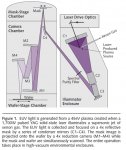
The company [Cymer] is developing the next generation of laser systems that will allow semiconductor manufacturers to produce even smaller, more powerful chips. Cymer recently showed off its technology, called Extreme Ultra Violet, in demonstrations.
Quote:
Cymer has two competitors pursuing rival systems, but neither is as well funded as Cymer, which today is the market leader in laser systems used in chip plants.
The company expects to deliver its first EUV system to its main customer for testing by year end.
The Next Generation of Semiconductor Manufacturing
Quote:
Today, only the most advanced chips are being produced using a 28-nanometer manufacturing process . . .
Cymer’s EUV lasers would enable 14 nanometer chip production initially and scale down to six nanometers or less eventually.
Posted on April 3, 2012 in EDA 360 Insider
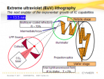
What Are the Challenges of EUV Lithography?
Quote:
Twelve years ago in 2000, Keith Diefendorff wrote about EUV lithography extensively in a very detailed Microprocessor Report article titled “Extreme Lithography.” Diefendorff detailed many of the same challenges still being faced today by EUV researchers and placed a timeline in that article showing production tools for EUV lithography being delivered in late 2005. That prediction turned out to be wildly optimistic. Goering’s blog post reports that IBM now expects that date to now be some time in 2013, about eight years later than predicted in Diefendorff’s article.
The following is quite a detailed bit of a technical read for sure; however it might be of interest to those that have been following the progress (or lack thereof) for EUV technology developments:
Intel Backs EUV for Next-Generation Lithography -By Keith Diefendorff {6/19/00-01}
Quote:
. . . drawing 70nm features onto an integrated circuit is the equivalent of drawing features the size of a quarter onto the surface of the earth from the height of an orbiting space shuttle—190 miles.
________________________________________
Posted on Friday, April 25th 2012 in U-T San Diego
San Diego Company Accelerates Spending On Next Generation Technology
Quote:
The company [Cymer] is developing the next generation of laser systems that will allow semiconductor manufacturers to produce even smaller, more powerful chips. Cymer recently showed off its technology, called Extreme Ultra Violet, in demonstrations.
Quote:
Cymer has two competitors pursuing rival systems, but neither is as well funded as Cymer, which today is the market leader in laser systems used in chip plants.
The company expects to deliver its first EUV system to its main customer for testing by year end.
The Next Generation of Semiconductor Manufacturing
Quote:
Today, only the most advanced chips are being produced using a 28-nanometer manufacturing process . . .
Cymer’s EUV lasers would enable 14 nanometer chip production initially and scale down to six nanometers or less eventually.
Posted on April 3, 2012 in EDA 360 Insider
What Are the Challenges of EUV Lithography?
Quote:
Twelve years ago in 2000, Keith Diefendorff wrote about EUV lithography extensively in a very detailed Microprocessor Report article titled “Extreme Lithography.” Diefendorff detailed many of the same challenges still being faced today by EUV researchers and placed a timeline in that article showing production tools for EUV lithography being delivered in late 2005. That prediction turned out to be wildly optimistic. Goering’s blog post reports that IBM now expects that date to now be some time in 2013, about eight years later than predicted in Diefendorff’s article.
The following is quite a detailed bit of a technical read for sure; however it might be of interest to those that have been following the progress (or lack thereof) for EUV technology developments:
Intel Backs EUV for Next-Generation Lithography -By Keith Diefendorff {6/19/00-01}
Quote:
. . . drawing 70nm features onto an integrated circuit is the equivalent of drawing features the size of a quarter onto the surface of the earth from the height of an orbiting space shuttle—190 miles.
Attachments

Last edited:


