IgorT said:[quote author=chimo link=1194375801/120#124 date=1203094834]I think I may have to pick up some to play with. Looks like a versatile little chip.
That's great. If more of us play with it, one should get it right sooner or later..
I mean, i'll try my best, but my bet is on you two...
") Then i'll just try to replicate the results.
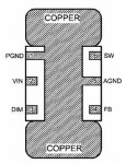
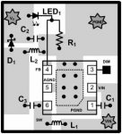
Then i'll just try to replicate the results.On the other hand, the 3410 has a circuit in the datasheet, that is pretty much perfect for driving a LD from a single cell Li-Po (Design example 6).. All it needs is two 4.7uH inductors. It's the circuit i posted a page or two ago.
Since almost all the requirements match, i'll just use the recommended parts and hope for the best.[/quote]
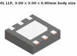
Did you find any in a SOT23 package or are they just available in the LLP?