Welcome to Laser Pointer Forums - discuss green laser pointers, blue laser pointers, and all types of lasers

LPF Donation via Stripe | LPF Donation - Other Methods

Links below open in new window

ArcticMyst Security by Avery

Anyone know eagle?

airy52

0
Joined
Jun 14, 2008
Messages
231
Points
0
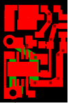
I made a pcb and laid it out pretty well in eagle. Pics below. Would anyone consider doing some of this for me, I cannot make the traces bigger, or else I run into clearance problems with my small tps chip. I like how woop and some people do the whole board copper and just etch out little pieces. Plus these traces are too small for 400 ma current IMO. I also need to space the traces farther from the pads. Will someone help me, do it for me, or teach me? PM me and I'll share the files.

layout.jpg


Joined
Sep 1, 2007
Messages
1,591
Points
0
Airy if i may suggest, Use express pcb its easier, eagle, if you really want to use it google eagle cad tutorials, Its hard at first but then you get it.
 

woop

0
Joined
Nov 9, 2007
Messages
342
Points
0
to make more copper area, i just go over the traces using the copper area tool, which draws rectangles.
you will want as much copper area connected to the ground of the TPS, as its heatsink.
to make the traces bigger, when you click the trace tool, at the top there is a drop down box with different widths. you can make some traces larger without affecting the ones to the TPS
eagle is hard to use and its really annoying sometimes, because there are small things about it which don't really make sense. But once your used to it its good, better than any other program i can find which does the same thing
 

airy52

0
Joined
Jun 14, 2008
Messages
231
Points
0
toked, i used express pcb for about 2 days. eagle is much much better. if you are less experience with computers though express pcb is probably for you. eagle is harder and has its problems, but the auto route feature and mix of complexity and simplicity are really nice. This board would have been very hard without autoroute. Makes it much easier to move parts around and around and around to make it perfect. :D Thanks woop I'll try that.
 

airy52

0
Joined
Jun 14, 2008
Messages
231
Points
0
Anyone see any improvements i could make before i go and print and etch this?
layout2.jpg
 
Joined
Oct 26, 2007
Messages
5,438
Points
83
Have you gone through Sparkfun's tutorial?  You can manually set the trace sizes and all that good stuff and then autoroute.  More tricks. For your problem, one thing to try is to make a special part that has the landing pattern pre-built for use with larger traces. Kind of like a break-out board.
 
Joined
Sep 1, 2007
Messages
1,591
Points
0
Yea I knowairy eagle is better, express pcb is easier for the novice, I use them both but i prefer expresspcb.

An example of a express pcb circuit for the tsp61200 attached.
Its made with the opamp, i modeled it after woops board
 

Attachments

  • boost_001.PNG
    boost_001.PNG
    5.7 KB · Views: 172

airy52

0
Joined
Jun 14, 2008
Messages
231
Points
0
yes i read those threads. I have a much different schematic. sorry.
 

woop

0
Joined
Nov 9, 2007
Messages
342
Points
0
airy52 said:
yes i read those threads. I have a much different schematic. sorry.
yours looks pretty much the same, but with an extra resistor and pot.
did you use the square tool in that last layout to make diagonal traces?
not the way to do it ;) try using the polygon tool. to make it fill in you have to link the polygon to another signal by changing the same to make it match.
 

airy52

0
Joined
Jun 14, 2008
Messages
231
Points
0
I couldnt get it to work. it only made dashed lines. you seem to have tried to explain how to do it but i dont understand. how exactly do i use the polygon tool correctly... Thanks woop!
 
Joined
Sep 1, 2007
Messages
1,591
Points
0
Oh Airy, forgot to tell you, preheat your
copper board with your iron before the transfer and it will come out perfect.
 

woop

0
Joined
Nov 9, 2007
Messages
342
Points
0
airy52 said:
I couldnt get it to work. it only made dashed lines. you seem to have tried to explain how to do it but i dont understand. how exactly do i use the polygon tool correctly... Thanks woop!
it sounds like you almost have it if its filling with hatched. there are two buttons at the top when you use the polygon tool, one is a hatched polygon, the other is a solid polygon. just click the solid one before you use it
 

J_Dogg

0
Joined
Jun 21, 2008
Messages
12
Points
0
airy52,
I used Pad2Pad. It has the auto route. I have Eagle and Express, and I like the Pad2Pad the best.
You can set the trace size and draw your own if you need a heat sink type pad.
I like Eagle, but its notto user friendly when youarea building a board and want to kick it out quick.... Also
Pad2Pad is a free d/l
J


Top